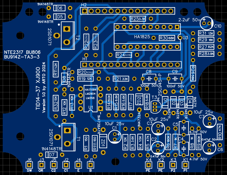
As an owner of a XJ900F, I have had my share of ignition problems as the bike ages and parts become scarce. I decide to dig deep and rebuild the PCB board of my ignition unit, I have way too many times replaced bits and the PCB board has become a mess. So here is my version, you must use the HA1825 and the HSA-10(B) board from the original. I have not done the mod yet, it will be sometime by the end of 2025 before I rewire the Bike, so “caveat emptor” if you decide to do this yourself from my information here (there might be some errors, who knows yet? it might just be absolutely correct.).
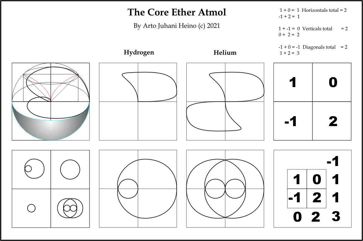
As I was searching my files for my next volume, I found my schematic for the Etheric Atom, the smallest resonant unit built from the Ether, it has no electrons or protons or even a nucleus, it has the super fluidic state of the Universal Ether. Any polarity created is solely due to its geometry, not to some fictitious particle that Modernism has concocted, nature has built the Universe from simplicity not complexity, I hope this is enlightening, regards Arto.
When you are designing binary circuits you will need to display your results in Decimal so it readable by the user, such as Temperature, Distance and Arithmetic calculation results. There are 74LS chips that will make the conversion for you, such as the 74LS148. It seems like we need to investigate the Ternary version and see if reveals some interesting results.
1A
The first design (1A) utilises the well known Ternary TAND Gate, where the assertions are the positive voltage only.
1B
The second design (1B) replaces the TAND with a TONLY Gate as we have no need of the negative values if we are interfacing a binary circuit. Looking at the TONLY Gate it seems that we do not need such a complex gate as the ones used, maybe we could just use some Unary Gates to do the same job.
1C
Design (1C) fulfils this completely using only 3 Unary gates, by creating a USR Gate that can be modified by another input, in this case it is the positive that gets asserted from the result of the first input, the final Gate is just another cascade from the second Gate. The output is either positive or zero so it can be linked to a Binary circuit.
1D
The last design (1D) in this set reduces the Unary Gates to 2, thus allowing a negative as an output, this is mainly for use in other Ternary circuits, like the one I will show in another design (2B).
My basic approach to using Ternary, is to make it more useful than binary which has many short falls that nobody can see unless you have been involved in designing these circuits from scratch, the current pardigm requires a complex binary arch to acomplish results and requiring multiple iterations to arrive at a result. Where Ternary can accomplish more in less gate interations than binary. Each Ternary Gate is only slightly more complex than its Binary counterpart, such as the inverter.
These circuits show how much can be achieved with less resources while being less complex connections than the binary version.
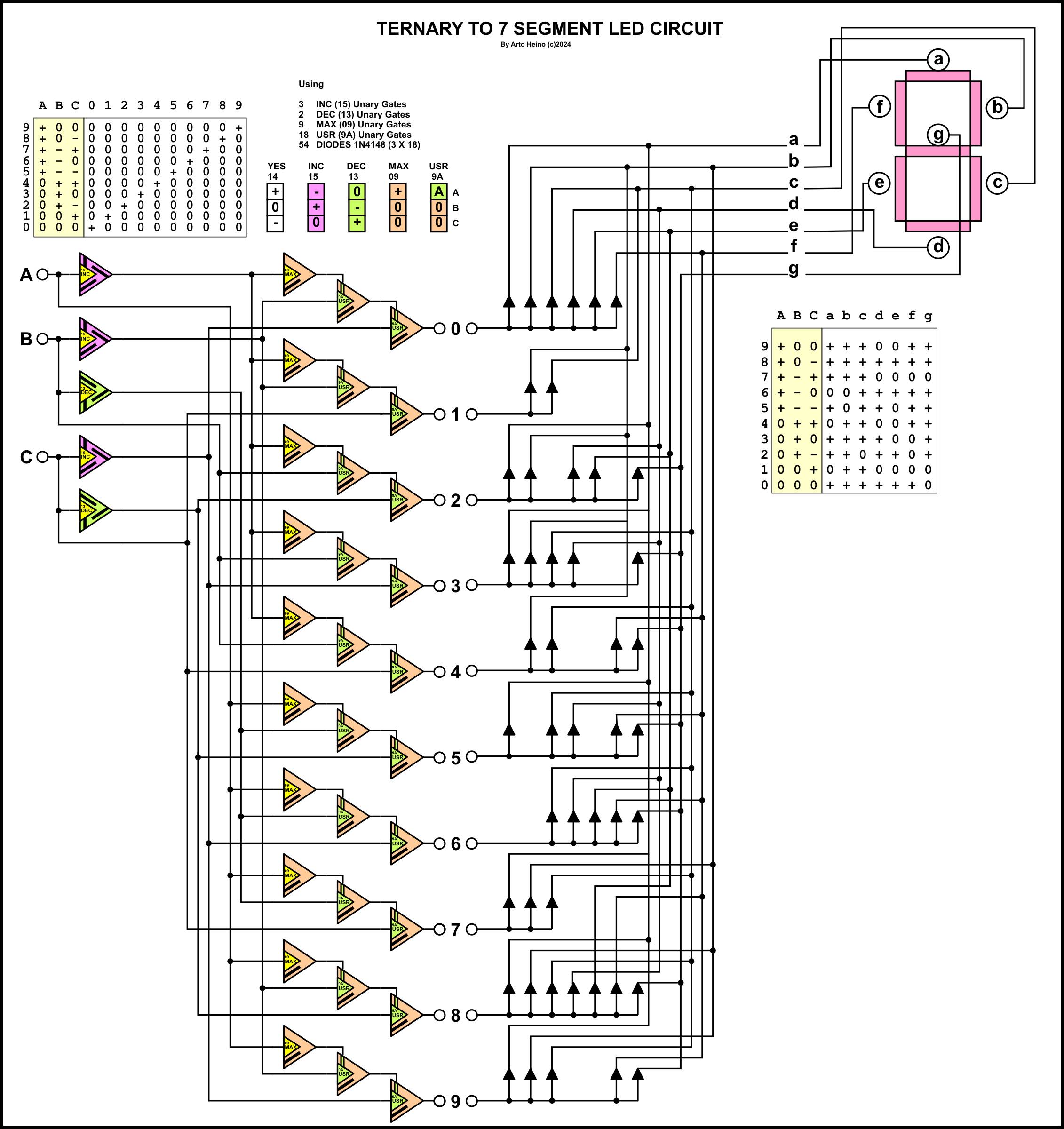
7 Segment Circuit
The final section is the Ternary to 7 Segment circuit. The first circuit (2A) is a basic 0 to 9 Led from a 3 Trit input, using the 3 Unary Gate logic from my earlier design (1C), the second circuit (2B) gives you another 9 more selections. Ternary easily uses negative numbers to increase data width selection, more elaborate schemes could be accomplished, like a complete 27 symbol choice, if I used all 13 positive numbers and all 13 negative numbers and zero.
2A
2B
Both of these designs use Diodes to accomplish the 7 Segment interface, making it suitable for a LED chip such as a Common Cathode TOS5121AR (Titan), LSD505400 (PlusOPTO), LTS-5003AWC (LITEON). You could even make your own with Leds or use a Large display.
I hope to finish my Division section of my Ternary ALU very soon, so far I have Addition, Subtraction, Multiply and a few Logic gates. I am still designing the shift registers and memory, while the ROM will be programmable with switches, I am basing it on 81 Trits at present.
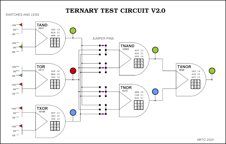
This board design concentrates on the 2 input Ternary Combinations.
I had made many Ternary Gates, here are 2 preferred designs using optical relays, using a 28 pin form.
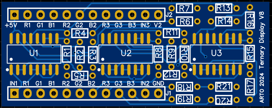
The display units are less demanding and can be designed in many ways, here are 3 designs, using 24 pins.
The V9 Ternary display unit requires 100 ohm resistors before grounding, if you use V7 or V8 you can just use shorting wires if you requires them, or just leave in the 100 ohm resistors. ( untested)
First of all the 6 switched inputs relates to three 2 input gates which are arranged to give you a maximum of choice.
The first 2 inputs A1 + B1 are directly combined in C1 to create the 2 output gate, designed by the links you combine in 12 pin matrix on the right side of each TNG2-1 chip.
To make your life easier I have put a number of gates that you can use on the bottom of the main board.
The LED outputs are in three groups:
1] switched inputs (6) A1 B1 A2 B2 A3 B3 2] output from each ternary gate (3) C1 C2 C3 3] output from combinations of 3 ternary gates D1 D2 4] output from the last 2 gates E1
To understand the Ternary Gate link matrix, here is a legend:
The jumper settings allows 81 variations, in 3 blocks -1 to 27, 28 to 54, 55 to 81;
I set the basic set up as number 67 from the list above. There are only 36 link combinations that include all three outputs from gates C (they form a top/bottom symmetrical list). Here are the sets:
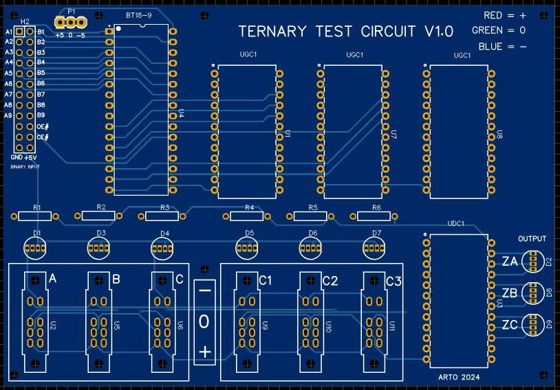
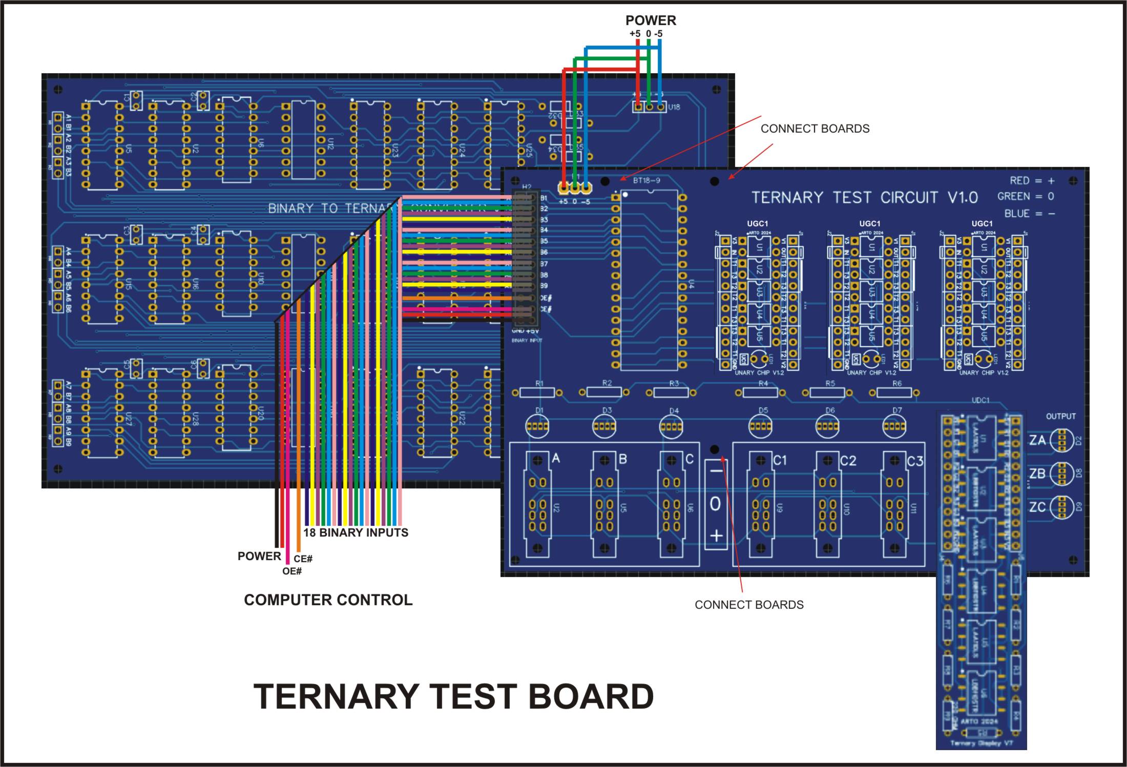
This board can accommodate 3 ternary chips the “BT18-9”, “UGC1” and “UDC1”, all of which are separate units, the BT18-9 needs either a set of ribbon cables with a socket or it can be directly connected with some HDR pins such as the connection diagram into the test board.
BT18-9
18 Binary paired Inputs (A1 B1) to (A9 B9) 9 Ternary outputs T0 to T8 OE# = output enable (you can set inputs then set to 0) CE# = chip enable (you must enable to 0 to start chip) +5V GND -5V
UGC1
1 Ternary input 1 Ternary output 1 led indictor of (-) 6 sets of programable inputs, in order
T1 T2 T3 T2 T3 T1 T3 T1 T2
T1 T3 T2 T2 T1 T3 T3 T3 T1
You can only connect 1 set at any one time, if you use a set of 3 jumper pins on all of the sets you could swap your combinations. These combinations will change your inputs into any one of six possibilities. This could also be done by using a analogue chip in a separate circuit.
UDC1
3 Ternary inputs 3 sets of 3 colour led outputs 3 sets of 3 colour led outputs (mirror of 1st set) So you could use these as Binary output switches or sensors as required. GND V1 = +5V V2 = spare 1 (-5v)
There are 3 ternary input switches (A B C) for all three RGB outputs (ZA ZB ZC) to function, there are also 3 selectors that need to be programmed first. Two of these are programmable by a binary source, while the other is by the onboard switches (C1 C2 C3). The current footprint of the display chip is 24pin pdip, even though the board is longer. As this is still only version 7, more work to do yet and I will eventually make it fit inside the boundary similar to the UGC1 board, on version 8 or 9. I am using optical relays in this design, something that I found useful in my ternary work.
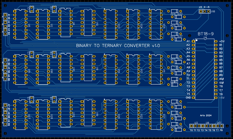
Starting from a Binary input where you have 2 bits to make a ternary trit:
00 = + 10 = 0 01 = –
The bit combination “11” is not valid and will not be used even though it is available as a binary output. The ternary converter ignores it.
Here are the 27 Unary gate combinations that are available and the binary combinations that will create them all. The UGI is the “Unary Gate Index”, numbering of all the gates in a system I have shown on my previous blogs.
Starting with the A1 and B1 as the first pair, then the A2,B2 then A3,B3, these three sets will give you a Unary set of 3 that will configure the basic Unary Chip “UGC1” to one of the 27 gates.
The second set A4,B4 + A5,B5 + A6,B6 will configure the next UGC1 gate. The third set are the switches C1,C2,C3 these will give you another UGC1 gate for you to use.
The outputs ZA,ZB,ZC correspond to the input data A,B,C, where your programmed UGC1 gate is being used to compute your result into the Z Led outputs. Where:
Red = + Green = 0 Blue = –
The input switches A,B,C,C1,C2,C3 also have RGB LEDs.
I hope this might start your interest in Ternary Logic and Computation, regards Arto.
** I have added UDC1 V8 to the Zipfile **
Ternary Test Boards PCB1D Zipfile
Al the PCB and Schematics for this project.
EasyEDA files only.
As a hobbyist I am always trying to work out how certain technologies function, so I decided to look into the PAL, PLA and any programmable logic arrays. So instead of using them as most technicians do I decided to create my own, by standard logic gates and switches, as I am just as interested in the why as the how.
These are my versions of Programmable Logic Arrays based on 74LS chips and 2 position toggle switches. I could try and replicate a standard PAL or PLE chip, but that would just clutter my simple approach as a learning tool. I made them so you can jumper the IC socket into to an existing circuit to test your programming.
LPA-4H10
Using AND/OR arrays, the AND array is either on(throughput) or off(made high) and the OR array is a fixed set to give you the maximum of multiple of outputs (6). My design is based on four 8 input AND gates, which are selectable by 8 switches, giving you a maximum of 32 switches. Using the 4 input bits and it’s inversion to give you 8 internal inputs for each AND gate.
IN1 x IN1# x IN2 x IN2# x IN3 x IN3# x IN4 x IN4# = OUTA1
Your input IN1 to IN4 are you only inputs, all the logic combinations are after your initial input.
AND Gates
2 INPUT, where A=INv and B=INw and Z=OUTAy (v = 1 to 4, w = 1 to 4, y = 1 to 4 )
AND NOT NOT AND AND AFBT ATBF NOR A B Z A# B Z A B# Z A# B# Z --------- --------- --------- --------- 0 0 0 1 0 0 0 1 0 1 1 1 0 1 0 1 1 1 0 0 0 1 0 0 1 0 0 0 0 0 1 1 1 0 1 0 1 1 1 0 1 0 1 0 0 0 0 0
3 INPUT
A B C Z A# B C Z A B# C Z A B C# Z ------------------ 0 0 0 0 0 0 1 0 0 1 0 0 0 1 1 0 1 1 1 1 1 0 0 0 1 0 1 0 1 1 1 1 1 1 0 0 1 1 1 1 1 1 1 1
A B# C# Z A# B# C Z A# B C# Z A# B# C# Z ------------------ 0 1 1 0 1 1 1 1 0 1 0 0 1 1 1 1 0 0 1 0 1 1 1 1 0 0 0 0 1 1 1 1 1 1 0 0 1 0 1 0 1 0 0 0
The abbreviations AFBT and ATBF was devised by me to simplify some of the less known logic gates that are available to the binary combinations. All these odd types of gates can be created with AND, OR, XOR, NOR, XNOR or NAND gates with an inverter on one of the gates as well. I don’t know how useful my ideas are to those Engineers who were educated in Digital Logic, but as an intuitive tool that I have developed, it has given me an insight into applying digital Systems to my Ternary work. As Ternary logic has a massive (19683) number of 2 input elements, your mind boggles at the idea of “Truelean Logic” as opposed to “Boolean Logic” which has only 16 two input elements. Here is the Matrix I developed when I sorted my relay logic elements, it clearly shows how it was developed.
AFBT (AfBt)
Z = (A = False = 0) + (B = True = 1) = True = 1 Z only equals True when (A = False = 0) and (B = true = 1) all the rest are False = 0. If you look at the A input as inverted you will have the same as standard logic, as such:
My Symbol: ____ A ----\ \ | \---------- Z B ----/____|
De Morgans Symbol2 Gated Logic _____ _____ A ----O| \ A ---|>O--| \ | |------- Z = | |--- Z B -----|_____/ B --------|_____/
ATBF (AtBf)
Z = (A = True = 1) + (B = False = 0) = True = 1 Z only equals True when (A = True = 1) and (B = False = 0) all the rest are False = 0. If you look at the B input as inverted you will have the same as standard logic, as such:
My Symbol: _____ A ----\ | | /---------- Z B ----/___/
De Morgans Symbol2 Gated Logic _____ _____ A -----| \ A --------| \ | |------- Z = | |------ Z B ----O|_____/ B ---|>O--|_____/
My Symbolism for multiple inputs
AfBCDEFGt

           *     *     *     *     *     *
Z = (A=0)+(B=1)+(C=1)+(D=1)+(E=1)+(F=1)+(G=1)=1

ACDEFGtBf

     *           *     *     *     *     *
Z = (A=1)+(B=0)+(C=1)+(D=1)+(E=1)+(F=1)+(G=1)=1

ABDFGtCEf

     *     *           *           *     *
Z = (A=1)+(B=1)+(C=0)+(D=1)+(E=0)+(F=1)+(G=1)=1
LPA Logic
The output from the AND array goes into a OR array that is set by 2 inputs using a OR combination, such as:
As you can see there are no more possible combinations than these six for a 2 input OR gate. Another added output is the ANDed output before the ORing which gives you another 4 outputs to use, giving you a total of 10 outputs.
Example 1a:
Here are the equations you can use, by using only IN1 and IN2 as your inputs:
So if you use two inputs, also using only 2 switchs F1 ans F2 of both inputs. Thus you get:
“#” = inversion
“^” = high = 1 (off)
OUTR1 = ((IN1 x F1) x (IN1# x F2^)) + ((IN2 x F1^) x (IN2# x F2))
When a switch “F” is on, then it equals the “IN” input. If “F” if off the it is high (=1).
If, IN1 = 1/0 and F1 is on and F2 is off (1), the rest of the switches are off (1) IN1(F3-F8). Every even switch uses the inverted version of the odd input going to the internal OR inputs.
also, IN2 = 1/0 and F1 is off (1) and F1 is on, the rest of the switches will be off (1) IN2(F3-F8)
IN1(F2) IN2(F1) = switch to high
             AND				OR
             _____
IN1 -0101---|  F1 \  	0101	             ______
            |      |------- OUTA1 ---0101 ---\      \
IN1 -0101--O|__F2_/ 	1111	              |      \
                                              |       \__OUTR1_1101
             _____		              |       /
IN2 -0110---|  F1 \  	1111	              |      /
            |      |------- OUTA2 ---1001 ---/______/
IN2 -0110--O|__F2_/ 	1001
This will give you output to the OUTR1 line, the OUTA1 and OUTA2. This is the output when you swutch IN1(F2) and IN2(F1) to high;
If IN1 = 0 and IN2 = 0 then OUTR1 = 1 , OUTA1 = 0 , OUTA2 = 1 If IN1 = 1 and IN2 = 0 then OUTR1 = 1 , OUTA1 = 1 , OUTA2 = 1 If IN1 = 0 and IN2 = 1 then OUTR1 = 0 , OUTA1 = 0 , OUTA2 = 0 If IN1 = 1 and IN2 = 1 then OUTR1 = 1 , OUTA1 = 1 , OUTA2 = 0
Where switch position “on” allows your input to go through the circuit, while “off” is only “high” (1) so the AND gate now is one less than your total maximum of 8. So if you switch all 8 to “off” this input will be only be a “1”, giving you a “1” on the input to one of the set OR matrix inputs.
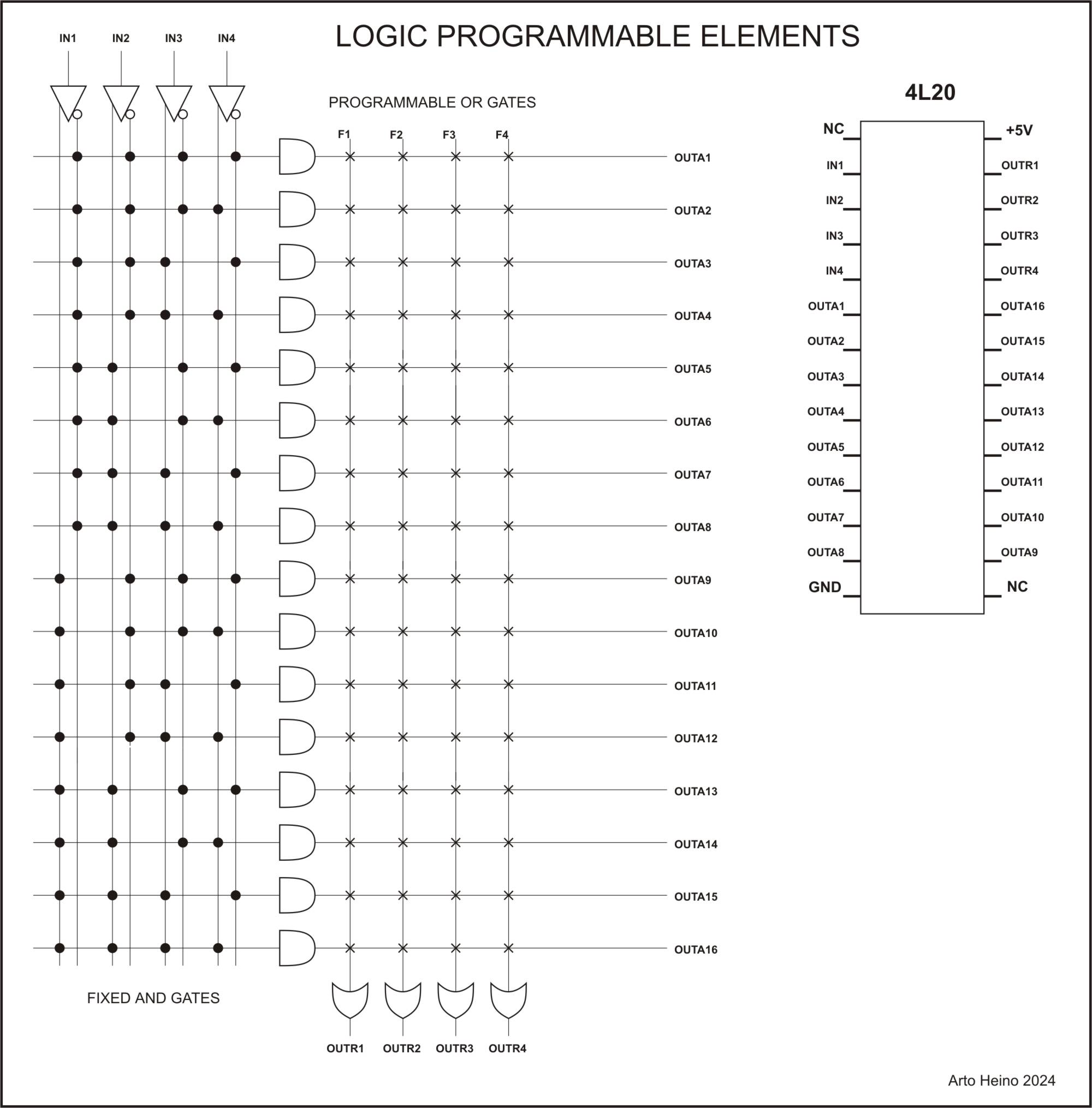
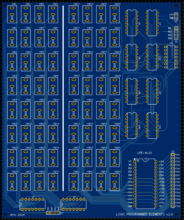
LPE-4L20
You get 4 inputs plus its internal inversions giving you 4 outputs (ORed) and 16 AND combinations. The off switch position is low, thus negating it throughput.
X = input o = inverted input
My first AND Matrix;
1 2 3 4 5 6 7 8 9 1 1 1 1 1 1 1
                  0 1 2 3 4 5 6
x x x x . x x . x . . x . . . .
. . . . o . . o . o o . o o o o

x x x . x x . . . x x . x . . .
. . . o . . o o o . . o . o o o

x x . x x . . x x . x . . x . .
. . o . . o o . . o . o o . o o

x . x x x . x x . x . . . . x .
. o . . . o . . o . o o o o . o
I was going to use this internal format, until I decided to use the standard PLE arrangement.
--------------------------------
   |   |   |   |   |   |   |
1 2 3 4 5 6 7 8 9 1 1 1 1 1 1 1		Net     AND Inverter output
                  0 1 2 3 4 5 6
. . . . . . . . x x x x x x x x   	H1  	A   1A
o o o o o o o o . . . . . . . .		U5_2	    1Y

. . . . x x x x . . . . x x x x 	H2	B   2A
o o o o . . . . o o o o . . . .		U5_4	    2Y

. . x x . . x x . . x x . . x x 	H3	C   3A
o o . . o o . . o o . . o o . .		U5_6	    3Y

. x . x . x . x . x . x . x . x		H4	D   4A
o . o . o . o . o . o . o . o .		U5_8	    4Y
So if you want to implement a 4 input XOR gate:
FnXOR = XOR (IN1 IN1# IN2 IN2# IN3 IN3# IN4 IN4#)
 =
(IN1 X IN2# X IN3# X IN4#) +
(IN1# X IN2 X IN3# X IN4#) +
(IN1# X IN2# X IN3 X IN4#) +
(IN1# X IN2# X IN3# X IN4) +
(IN1 X IN2 X IN3 X IN4#) +
(IN1 X IN2 X IN3# X IN4) +
(IN1 X IN2# X IN3 X IN4) +
(IN1# X IN2 X IN3 X IN4)
Switches used: (from 1 to 64) 5 9 17 29 33 45 53 57 – or – first column (1 to 16) 2 3 5 8 9 12 14 15 are ON all other switches are OFF
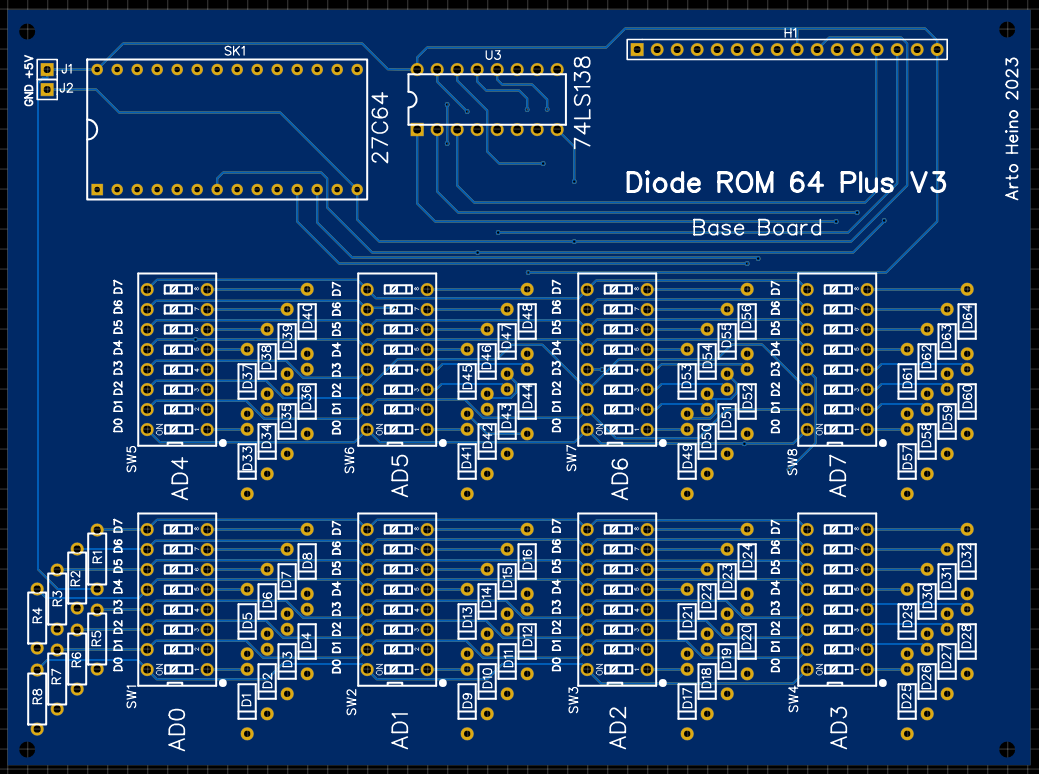
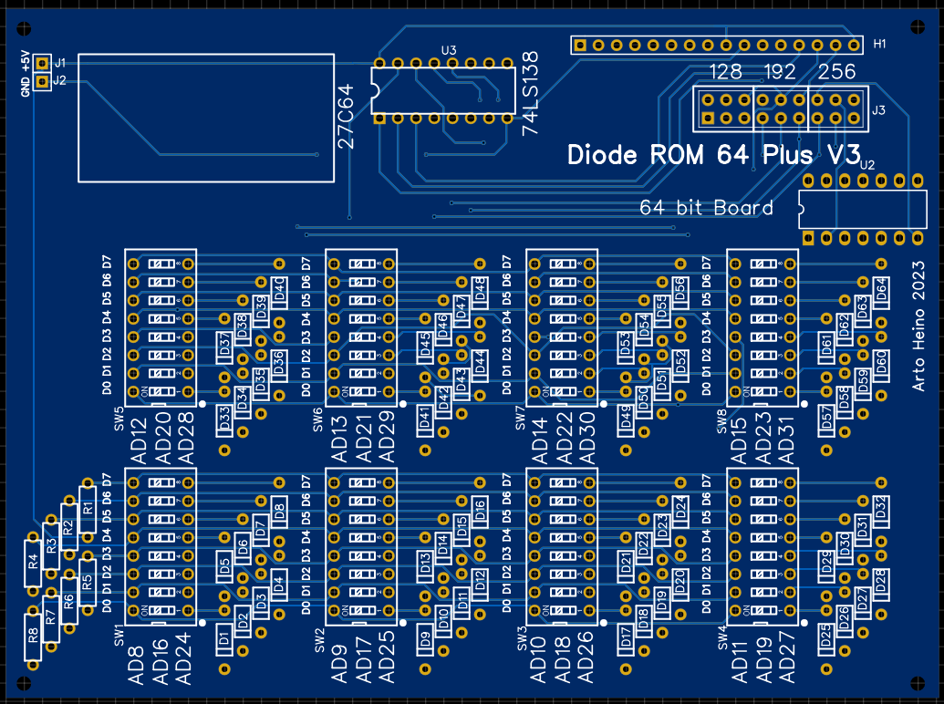
As my research moves along, I decided to create a Diode Memory unit first for binary use, before I implement the ternary memory version. I designed 2 types of boards, the first is the base board which is the first 64 bits or 8 bytes, the 2nd board can be stacked on top to create 128 bits or 16 bytes with more boards on top for 192/256 bits or 24/32 bytes. I will be building these soon, as these designs have not been tested yet, I suggest checking my work, I will confirm these in another blog.
The ROM choice was a 27C64 which is a 8Kx8 and is very popular, available in general stock and I will use it in further designs, the decoder is a 74LS138 which seems to be a great choice for this simple project. The only problem I had was the 138 has only 3 bits to decode, so I had to add a few extra bit of routing to create 32 bytes. The 138 has 3 enable lines GA_, GB_, G1, so the first block I put G1 high and GA_and GB_ would be enabled when both are low, these are from the A3 and A4 lines which are low. The second block I put GA_ low to ground with GB_ and G1 would be A4 as low and A3 as high. As you can see by the diagram I swapped A3 and A4 with GA grounded for the 3rd block, the last block I used an inverter on GB_ from A3 which must be high,
If you are not using 32 bytes then you can ignore the 74LS04 connection. To use each block you must bridge the labelled connectors with jumpers. The Parts list for 2 boards are:
SK1 = 28 pin DIP socket with extended legs
H1 = 16 Pin socket with extended legs x 2
U3 = 74LS138 x 2
R1-R8 = 10K resistors x 2
D1-D64 = 1N4148 Diodes x 2
SW1-SW8 = 8 sw DIP x 2
J1-J2 = Pin for Power x 2
Each corner has 2mm holes , add crews and extended legs as needed x 2
If you choose to build it, you will be limited to 32 bytes. To test the unit you could plug it into to a EPROM reader. My next version should allow up to 256 bytes or more. Regards Arto.
Diode ROM PCB1C Zipfile
All the PCB and Schematics for this project. EasyEDA files only.
To start the journey of discovery, we must have all the building blocks and tools ready to use as creativity requires a selective group of useful mechanisms to achieve a modicum of feed back to keep the momentum going forward towards interesting and useful discoveries. The Ternary building block are here, along with a Binary controller that you can use to design your Logic elements as needed. I have shown previous Unary gates and they are still usable in these designs. I decided to put 4 gates in one unit so wiring can be simplified when you create the 2/3/4 input gates. For a 2 input gate you need 3 gates for the columns and a summing gate and 3 gates for the rows a summing gate for the rows and the result. This makes it simpler, you will only need 2 unary boards for an 2 input gate, a base board was designed to make this easier, these can be stacked, as high as required.
Parts List for each Unary Gate V6
U1,U3,U4 _________G3VM-353A U2,U5 ____________G3VM-61A1 U6,U8,U9 _________G3VM-353A U7,U10 ___________G3VM-61A1 U11,U13,U14 ______G3VM-353A U8,U15 ___________G3VM-61A1 U16,U18,U19 ______G3VM-353A U17,U20 __________G3VM-61A1 LED1,2,3,4 ________3mm Blue 36 x ______________Male/Female headers 20 x ______________4 Pin sockets (if required) 1 x _______________Unary Board V6
Parts List for Base Boards
4 x _______________24Pin Fmale Header 8 x _______________3 Pin
Parts List for Binary to Ternary Gate Selector Board
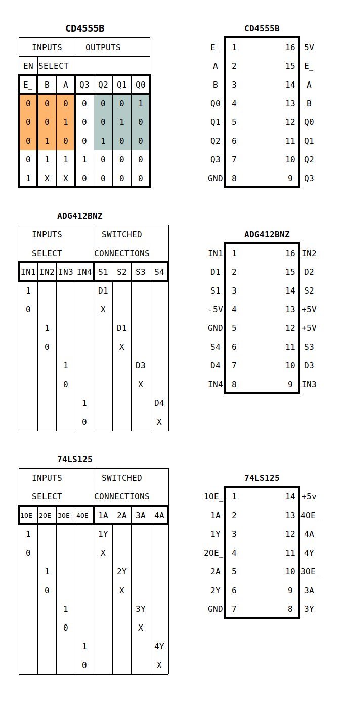
6 x _______________CD4555BE 9 x _______________ADG412BNZ C1,C2,C3,C4,C5,C6 _100 nF Caps D1-D12 ___________1N4007 D19,D20,D21,D22 __1N4007 1 x _______________LM7805 1 x _______________LM7905 C7,C10,C12,C22 ___47uF Electrolytic Caps Led1 _____________Led R1 _______________1K 3 x _______________6 Pin 3 x _______________5 Pin 15 x ______________8 Pin Dip 1 x _______________7 Pin Dip 1 x _______________74LS125
1 x _______________LAA110LS 1 x _______________LBB110STR 3 x _______________220 Ohm 3 x _______________1xPin hdrs 2.54 1 x _______________4 pin hdr 1.27 1 x _______________RGB PCB board
Parts List for TMS9995 Board
1 x ________U8 ____74LS138 1 x ________U5 ____74LS32 1 x ________U6 ____MAX232CPE 1 x ________U7 ____TMS9902 1 x _____U11+U12__TMS9901 x2 1 x ________U1 ____TMS9995 1 x ________U4 ____74LS04 1 x ________U3 ____62256-07 SRAM 1 x ________U2 ____M27C256 EPROM + Binary Data Cortex + Terminal 1 x _______________DB9 RS232 RA port 1 x _______________Header 6 Pin C1-C8 ____________100nF C11,C12___________100nF C16 -C20 __________1uF Electrolyticn R1________________10K R2 – R6____________1K C13, C14 __________15pF X1 _______________12 Mhz XTAL 1 x _______________LED21 LED indicator 1 x _______________SW4 Micro switch C15 ______________10nF 4 x _______________10 pin RA Male Pin Headers 1 x ________U9 ____LM7805 C22, C23 __________47Uf DC1 ______________9v input Jack 3 x________________40 Pin Dip 2 x _______________ 28 Pin Dip 2 x _______________ 14 Pin Dip 2 x _______________ 16 Pin Dip 1 x _______________ 18 Pin Dip 1 x _______________TMS9995 SBC PCB Board (Conner Stuarts Design)
Boards
Unary Gate Base Board V6 Unary Gate Base Board Singles V6 Binary to Ternary Gate Controller V1 Ternary Input Switches Ternary Bit Display TMS9995 SBC
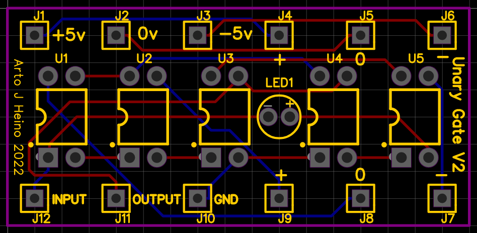
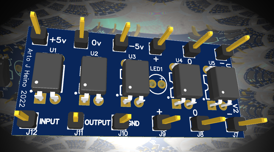
Each Unary board consists of 4 separate Unary Gates they can be used as a set or individually, depending which base board you use.
The Unary Gate Base Board has been configured as a 2 input gate A, B and the result in C.
The Unary Gate Base Board Singles is configured to use as either a 2 input gate by wiring it as required or as single chains or groups.
J1, J4, J7, J10 are your ternary inputs, while J2, J5, J8, J11 are your outputs to each gate.
K1, K2, K3 are configurable with J40, J39, J38 as a matrix to give you all 27 Unary configurations. The interconnections are configurable with a small 6 pin cross connected board, or you can use jumper cables if you choose.
Controller Board
This has a 12vac input and 18+3 pin binary input and a 3 pin ternary output. It was designed to connect to a TMS9995 SBC with CRU outputs and have software to control the gate configuration in hardware.
With Five Boards there are 45 binary controls which will give you a Ternary Multiplexer made of five 2 input gates and 3 Unary gates. Once you have tested and configured your logic, then you can use the base board with plugin matrix connectors as your final gate design.
Setting Your Bits
H1, H2 and H3 are your binary control bits to select each gate type. You select 6 bits to as either decimal or Hex to each unary port. I added U28(74LS125) and U29 3 pin header which is used to switch each gate on, under software control as required.
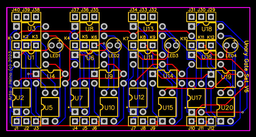
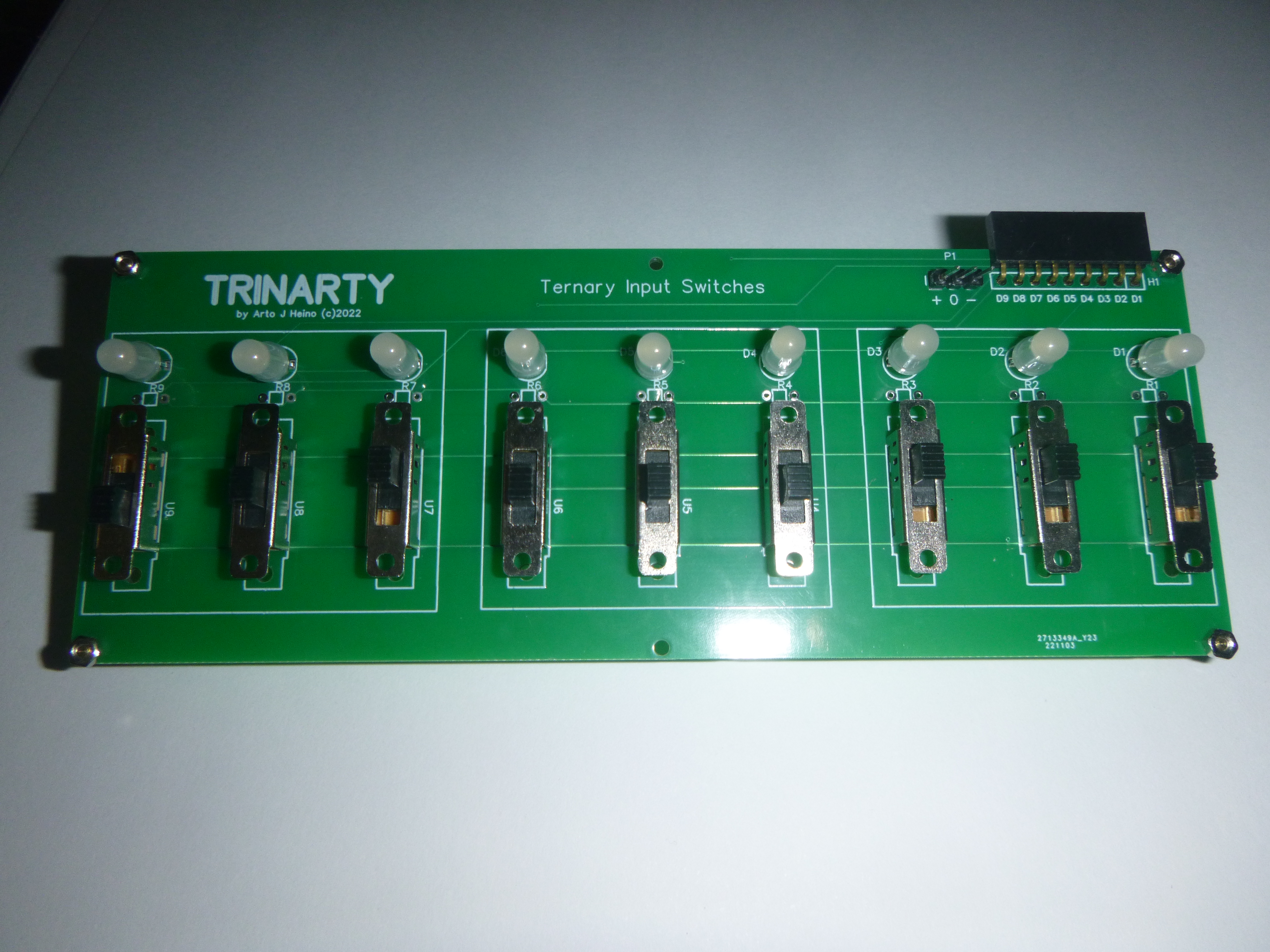
Ternary Input Switches
This board has 9 ternary outputs and can be used to control the A+B inputs on the Unary boards. There is 9 RGB indicators for the slide switches, Red = +5v , Green = 0v , Blue = -5v.
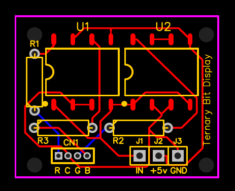
Ternary Bit Display
This small board gives you a visual indication of your output bits, Red = +5v , Green = 0v , Blue = -5v
Listed below is the Program to control the Ternary Gate Selector. If you want to attach more Selector boards you will need to expand the CRU outputs. I have left the header J5 to allow CE for more TMS9901 to be added at some point. The next version will also have have mounting board for 4 more chips, giving a total of 96 outputs.
Where 21 are needed for each 2 input gate, this allows control of 4 2 input gates, 84 pins , leaving you 12 spare pins for other controls.
This is a Cortex Basic program to control one two input gate.
8 REM TERNARY GATE CONTROL 9 REM *** BY ARTO HEINO 2023 ** 10 REM OUTPUT ON 9901 PORT BIT 0 to bit 20 (21 BITS) 11 REM TO CONTROL TERNARY 18 BIT GATES + 3 BIT CONTROL 12 REM 13 REM SETUP BASE ADDRESS OF 9901 to 64 decimal = >0040 HEX 14 BASE 64 15 DIM TR(27,6) 17 REM DISABLE EACH CD4555BE CHIP 18 CRB(16+18)=0 19 CRB(16+19)=0 20 CRB(16+20)=0 24 REM LOAD 27 TERNARY GATE BIT DATA 25 RESTORE 27 FOR Z=1 TO 27 28 FOR X = 1 TO 6 29 READ TR(Z,X) 30 NEXT X 31 NEXT Z 32 REM SELECT 3 GATES 33 FOR A=1 TO 3 36 PRINT “COLUMN “; A 38 PRINT “SELECT GATE 1 TO 27” 39 INPUT GT 40 IF GT<1 OR GT>27 THEN GOTO 38 42 FOR BT=1 T0 6 45 REM SET HIGH OR LOW 48 CRB(15+BT+(A*6-6)) =TR(GT,BT) 56 NEXT BT 57 NEXT A 60 REM ENABLE EACH CD4555BE CHIP 61 CRB(16+18)=1 62 CRB(16+19)=1 63 CRB(16+20)=1 64 END 65 REM DATA FOR GATES 66 REM H1 + H2 + H3 101 DATA 0,0,0,0,0,0 102 DATA 1,0,0,0,0,0 103 DATA 0,1,0,0,0,0 104 DATA 0,0,1,0,0,0 105 DATA 1,0,1,0,0,0 106 DATA 0,1,1,0,0,0 107 DATA 0,0,0,1,0,0 108 DATA 1,0,0,1,0,0 109 DATA 0,1,0,1,0,0 110 DATA 0,0,0,0,1,0 111 DATA 1,0,0,0,1,0 112 DATA 0,1,0,0,1,0 113 DATA 0,0,1,0,1,0 114 DATA 1,0,1,0,1,0 115 DATA 0,1,1,0,1,0 116 DATA 0,0,0,1,1,0 117 DATA 1,0,0,1,1,0 118 DATA 0,1,0,1,1,0 119 DATA 0,0,0,0,0,1 120 DATA 1,0,0,0,0,1 121 DATA 0,1,0,0,0,1 122 DATA 0,0,1,0,0,1 123 DATA 1,0,1,0,0,1 124 DATA 0,1,1,0,0,1 125 DATA 0,0,0,1,0,1 126 DATA 1,0,0,1,0,1 127 DATA 0,1,0,1,0,1
Here is the layout for the SBC and the Ternary Gates.
An alternative design without the SBC and just putting units together.
Here are a few pictures regarding some of the components.
This is the CODE for the 27 selections of Unary gates, H1,H2,H3 CRU outputs.
Here are the PCB’s for the Basic boards.
If you want to see more of this type of content, I would appreciate your support to help pay for more original designs and parts. I hope you enjoy this work, regards Arto.
Ternary PCB1A Zipfile
All the PCB and Schematics for this project. EasyEDA files only.
To be clear the multitude of Ternary 2 input gates is a gift to the creative mind, I have written a program that enumerates all 19683 and deemed all of them useful. An example of this is gate 2272 (TAB-index), which is “Tautology” or all “+1”, so any inputs at A and B results in +1 on the output. You might say what is the point of that? Only now it acts like a buffer or a line driver, so it serves a “function” in a ternary circuit or a re-encoder in a more complex circuit. After deciding what is needed to develop a Ternary computer, I first looked to the 27 Unary gates and the all gates that are commonly used in binary circuits, like AND, OR, NAND, NOR etc…which there are a total of 16 and which 6 are deemed the most useful.
Here is the complete set of Binary Relay Logic
Exploring the Trinary logic opens a whole new way of seeing and thinking about computer architecture. For example a multiplexer is a most versatile device when designing circuits so I chose to explore this device to see what can be learnt from applying ternary logic to its internals. In a previous post (https://artoheino.com/2021/05/04/the-2-to-9-decoder/..) I showed my crafted and workable TD2-9 (2 input to 9 output) decoder. this will be the starting point of some new discoveries.
First lets go back to the simplest version the TD1-3 decoder:
I chose this one mainly due to the fact it can be used to decode Ternary to Binary, so one input from a Trinary based system can produce 3 signals to control a Binary based chip. So a mixture of Binary and Trinary is not difficult to attain.
Here is an example of one of my Binary to Ternary Interfaces based on a Analog Devices chip.
I have used a spread sheet to design the small Unary modules and 2 input Ternary Gate modules to develop these designs, they were based on the Ternary Relay designs I have outlined in my previous work.
The spread sheet model has helped me in developing combinatoric circuits and ensure consistent logical flow, as this is a new technological playground and has some crude pointers and intellectual fences to overcome. As the diagram of the 2 circuits show, we can decode with positive or negative numbers without the binary load that is usually a constrictive affair and become overly complex.
After much mind bending Ternary Logic visual calculations and pattern recognition, here is the First Ternary Multiplexer, TM3-1 with a future TM9-2, TM27-3 and TM81-4 as simple extensions. Where as the Binary can only achieve 2-1, 4-2, 8-3 and 16-4, so imagine how versatile these gates can be.
With this TM3-1 you could create a Ternary to binary converter, by using two of these
A Binary to Ternary converter is also possible:
They can also be usable as a 2-2 Encoder in binary:
Also by cascading the TM3-1 you can create the TM9-2.
Choice of Unary Operators
Using the binary combination of AND plus OR gates, I first applied the binary equivalents of the Ternary gates to create the Multiplexer but found the Ternary logic would not cooperate as easily as binary. This is when I realised that the ternary system would have a simpler gate choice to achieve the same result. Instead of TAND I used SAND, which has a simpler matrix, while the DNOR is similar to the TNOR gate. This gave me the start, which later I found that VAND and LAND gates also work.
Ternary 2 input Gates
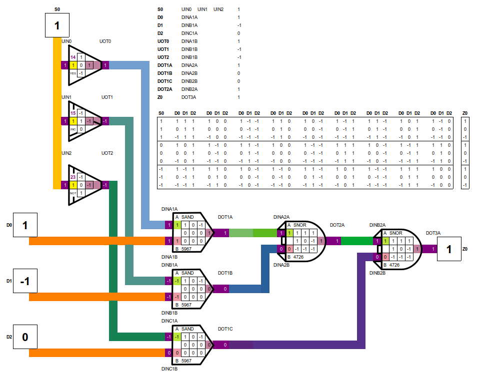
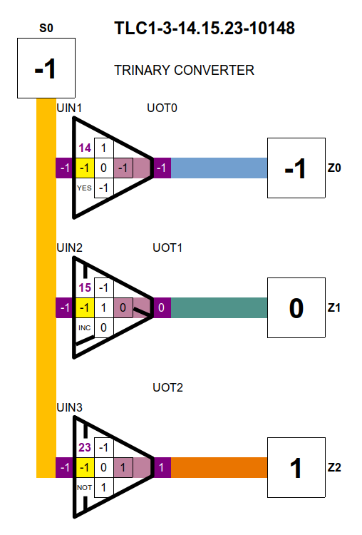
Ternary Converter
During these discoveries, I realised a ternary converter would be useful by itself. The numbering system describes the 3 gates and the 2 input equivalent.
Example:
TLC1-3-14.14.23-10148 TLC = Ternary Logic Converter 1-3 = 1 input 3 output 13.15.23 = Unary gates used 13, 15 and 23 10148 = The 2 input gate number equivalent 1 to 19686
Hardware Versions
After many attempts to make these circuits simple and easy to follow, I decided to concentrate on the relay versions but started using Photo-MOS Relays instead. This I found to be advantageous as the noise was eliminated and the current consumption decreased with the bonus of high speed. I would like to see a Photo-mos version of Programmable Logic, this would create a whole new industry, as the Photo-mos relays are already a mature technology today.
There are many manufacturers of Photo relays, lets look at the IXYS lettering, this will simplify your creative pallet. NO = Normally Open, NC = Normally Closed.
IXYS
LAA 2 in NO + NO 2 out 8 pin Dip
LBA 2 in NO + NC 2 out 8 Pin Dip
LBB 2 in NC + NC 2 out 8 Pin Dip
LCA 1 in NO 1 out 6 Pin Dip
LCB 1 in NC 1 out 6 Pin Dip
LCC 1 in NC + NO 2 out 8 Pin Dip
I opted to use the DIP 4 as well, as this would give me a more flexible layout and get different brand parts sourced and tested.
These designs cover the scope of mechanical relays, where you can configure SPST, SPDT, DTSP, DTDP different combinations, you can also have the current flow in either direction or as in neutral where there is no action to trigger the relayed combination.
in long hand: If A1 x 10 + A3 =11 then E2 Display Value = B1
Where you would normally write
If A1 = 1 and A3 = 1 then E2 Display Value = B1 By multiplying A1 by 10 then I can add the two the values without an a “AND” logical statement while keep track if it is true or not.
Example of A3 = 1 Say if A1 = 1 then A1 x 10 + A3 = 11 A1 = 0 = 1 A1 = -1 = -9
Also if A3 = 0 Say if A1 = 1 then A1 x 10 + A3 = 10 A1 = 0 = 0 A1 = -1 = -10
And finally if A3 = -1 Say if A1 = 1 then A1 x 10 + A3 = 9 A1 = 0 = -1 A1 = -1 = -11
So you can see that the “+” in the code means “OR” , so now you have a truth table with 9 unique values. -11 -10 -9 -1 0 1 9 10 11 .The pointers are the input at A1 and A3 which define the value at E3 , altogether these are the general Logic Inputs of A B result in C.
The code for the Unary input was much simpler.
= IF(A2=1,B1) + IF(A2=0,B2) + IF(A2=-1,B3)
As you can see it is vital that your two input gates are in the correct order where as the binary version does not have that problem. Your A and B inputs and the coding of your ternary signals have a specific order which is determined by the original Truth table orientation. The convention I call “Natural” (T1) is “+ 0 -” and the Truth table is “A” rows top to bottom and “B” columns is left to right. The other options, which I have found among other ternary researchers are listed here:
By this table you can see how this effects the look of the Truth Table. So as in human relations we also have different languages in communicating, translating will not be difficult as these ideas are universal. The Non-Balanced (0 1 2) might not be as easy, as these now become arbitrary according to the designer, they might consider the “switched P” (0 + -) used as “0 1 2”, where as the “Natural” being “+ 0 -” and the equivalent would be “1 0 2”, a very confusing translation would make it difficult. This ordering is related to the voltage levels from 0 volts to 1 volt to 2 volts, this would be articulated in hardware making it incomparable with the Natural order and only interfaced through a translator. The Natural system also easily accommodates the AC wave and can be used as a clock without much difficulty.
A Unary Gate Chip
The idea was to make a 12 pin bread board ready plug component that could be used to create gate combinations and test the results. Here is the UGC-V2 and a plug in header to change the Unary gate number as required. The plug-in header sits on top of the the J4 to J9 pins, it allows you to use all 27 gates. The unit is 20mm x 43mm and the plug is 20mm x 20mm.
Unary Gate Chip
I hope this spurs some interesting Ternary work and we might see a bright future in using “LIGHT” as the interface between the old Binary Paradigm to the new Trinary way of doing things. Regards Arto.
I had spent most of my childhood making observations that I had to verify, by testing if it was reality or some sort of an illusion, where most children do not remember having to apply their mind to the task as this is a natural process in all human beings. Where as I remembered a simplified version of this methodology and applied it to numerous optical and scientific illusions intuitively before I could even codify the process in writing as an adult. Much of what I had learned about what the Scientific Method is, was gleaned from extensive reading of countless journals, books and encyclopedia as I was growing up in my childhood, I cannot quote a professor or institute, only Sir Francis Bacon and my own personal life experience.
Historically Sir Francis Bacon(1561-1626) was the man who had codified the Scientific Method which was known in his time as the Baconian Method. Briefly the Scientific Method are steps that help scientists conduct understanding and clarity in the use of dynamic technology and material sciences, which is made up of seven main steps:
1 – State the problem, 2 – Research the problem. 3 – State your hypothesis, 4 – Do an experiment, 5 – Analyze data, 6 – Conclude the results, 7 – Form a conclusion.
Bacon also had devised what he called the idols of the mind, that could be called delusions or as he describes as false images. These four obstructions must be overcome to have a clear path of correct scientific reasoning. I have added a fifth as my way of addressing the intellectual dishonesty that has been foisted on our education system by the use of symbols.
Idols of the Tribe (Idola tribus) This is humans’ tendency to perceive more order and regularity in systems than truly exists, and is due to people following their preconceived ideas about things.
Idols of the Cave (Idola specus) This is due to individuals’ personal weaknesses in reasoning due to particular personalities, likes and dislikes.
Idols of the Marketplace (Idola fori) This is due to confusion in the use of language and taking some words in science to have a different meaning than their common usage.
Idols of the Theater (Idola theatri) This is the following of uncorrected dogma and not asking questions about the world.
Idols of the Symbol (Idola signo) This is the misunderstanding of visual mnemonics due to uncorrected use of symbols, conflating the symbol with a preconceived negative or positive outcome.
After a lot of thought of Bacon’s ideas, they revealed to me another view of our problematic interaction with our observations and rational framework. There is a way of seeing our limitations of reasoning and finding that they hold our life in a type of prison built from our needs or ideas within our existence.
Prisons of the Mind (Carcer Cogitatio) The imagined truth being our only limitations in our mind.
Prisons of Ideas (Carcer Notio) The ill defined and illogical ideas limiting our perceptions of reality.
Prisons of the Emotions (Carcer Motus) The uncontrolled reflexes within our emotive being.
Prisons of Sustenance (Carcer Victus) The essential and incessant need to maintain regulated nourishment.
Prisons of the Environment (Carcer Ambitu) The real need to have levels of protection from all forms of physical damage.
These prisons I have listed are very real to most people, they are just not aware they are inside them, while we can all agree that Sustenance and Environment are two that we are very intimately connected with but the others are no so obvious. The Mind Prison is simple to understand if you believe the Earth is flat, a limitation that is built from a lack of understanding and verifiable information. The Ideas Prison, is more related to our notions of politics, philosophy and poetry, where ideas have consequences to the passage of life, like the 120 million crucified in the 20th century for the flawed Marxist doctrines. The Emotions Prison, is by no means an easy hurdle to leap over as each one of us has either unfulfilled, exasperated or subjugated emotional issues to some degree, these we will render a mental cage to keep those feelings from destroying our lives.
The following definitions of the Scientific Method can be compared to text book versions and should be much simpler and clearer than most.
I have separated it into nine distinct headings, each can be considered recursive until it satisfies its criteria of application. These are my own versions, in the nine steps of the artists natural scientific method go something like this:
1 Observation of Interest Make an single observation or many observations.
2 Facets of Observation Ask questions about the observations and gather information.
3 Hypothesis Form a hypothesis, a tentative description of what has been observed, and formulate predictions based on that hypothesis.
4 Prediction Build the hypothesis with the predictions into an experiment that can be reproduced. Building a theory.
5 Analysis Analyse the data and draw conclusions; accept or reject the hypothesis or modify the hypothesis if necessary. Adjust theory to fit facts.
6 Experiment Physically reproduce the experiment until there are no discrepancies between observations and theory. Design for Replication of methods and results.
7 Variables Dependent and independent variables are brought to a reduced set and general formula are created. Simplification of formula and universality is the prime reasoning.
8 Conclusion Does it conform to the real world? Does it operate in a different environment or frame of reference?
9 Reality This is now a law of nature as described by man, simplified to its primal state and understood intrinsically by man in all frames of reference. The extended boundary of theory has been overcome, it is considered a fact.
This brings me the words and meanings of “Science”? Science is not a category of study, it is a process of inquiry with deductions. Science is a method not a vocation. When something is Scientific it means it can have the Scientific Method applied to it without difficulty and its conclusions adhere to its methodology. A Scientist is someone who apples the Scientific Method to an observation. A Professor of Science is someone who can apply the Scientific Method with expertise.
The implications of a “Theory”, firstly it must have self consistency, agreement with observations and have universal usefulness, alas, as it is only a theory as it only conforms to the first four of the steps required in the Scientific Method. Much of modern science is now “Theoretical”, they are trapped in the fifth stage and are given special compensation for digging up new “Theories”, creating a branch called “Theoretical Physics”. These are now a protected class defined by Cultural Marxism, as the real scientists who follow the Scientific truth and its complete Scientific Method are under the mercy of authoritarian political correctness and a false religion of “Scientism”.
An error has occurred; the feed is probably down. Try again later.
Join 130 other subscribers
Published material Link
Talking to the Birds
Book Available NOW
At Amazon
At Createspace
https://www.createspace.com/4513692
______________________
Cartoons
http://www.scribd.com/doc/106684504/Scraps-Sketches-and-Satire
_______________________
Magic Square
http://www.scribd.com/doc/33050524/The-Magic-Square-of-Three-Crystal