When you are designing binary circuits you will need to display your results in Decimal so it readable by the user, such as Temperature, Distance and Arithmetic calculation results. There are 74LS chips that will make the conversion for you, such as the 74LS148. It seems like we need to investigate the Ternary version and see if reveals some interesting results.
1A
The first design (1A) utilises the well known Ternary TAND Gate, where the assertions are the positive voltage only.
1B
The second design (1B) replaces the TAND with a TONLY Gate as we have no need of the negative values if we are interfacing a binary circuit. Looking at the TONLY Gate it seems that we do not need such a complex gate as the ones used, maybe we could just use some Unary Gates to do the same job.
1C
Design (1C) fulfils this completely using only 3 Unary gates, by creating a USR Gate that can be modified by another input, in this case it is the positive that gets asserted from the result of the first input, the final Gate is just another cascade from the second Gate. The output is either positive or zero so it can be linked to a Binary circuit.
1D
The last design (1D) in this set reduces the Unary Gates to 2, thus allowing a negative as an output, this is mainly for use in other Ternary circuits, like the one I will show in another design (2B).
My basic approach to using Ternary, is to make it more useful than binary which has many short falls that nobody can see unless you have been involved in designing these circuits from scratch, the current pardigm requires a complex binary arch to acomplish results and requiring multiple iterations to arrive at a result. Where Ternary can accomplish more in less gate interations than binary. Each Ternary Gate is only slightly more complex than its Binary counterpart, such as the inverter.
These circuits show how much can be achieved with less resources while being less complex connections than the binary version.
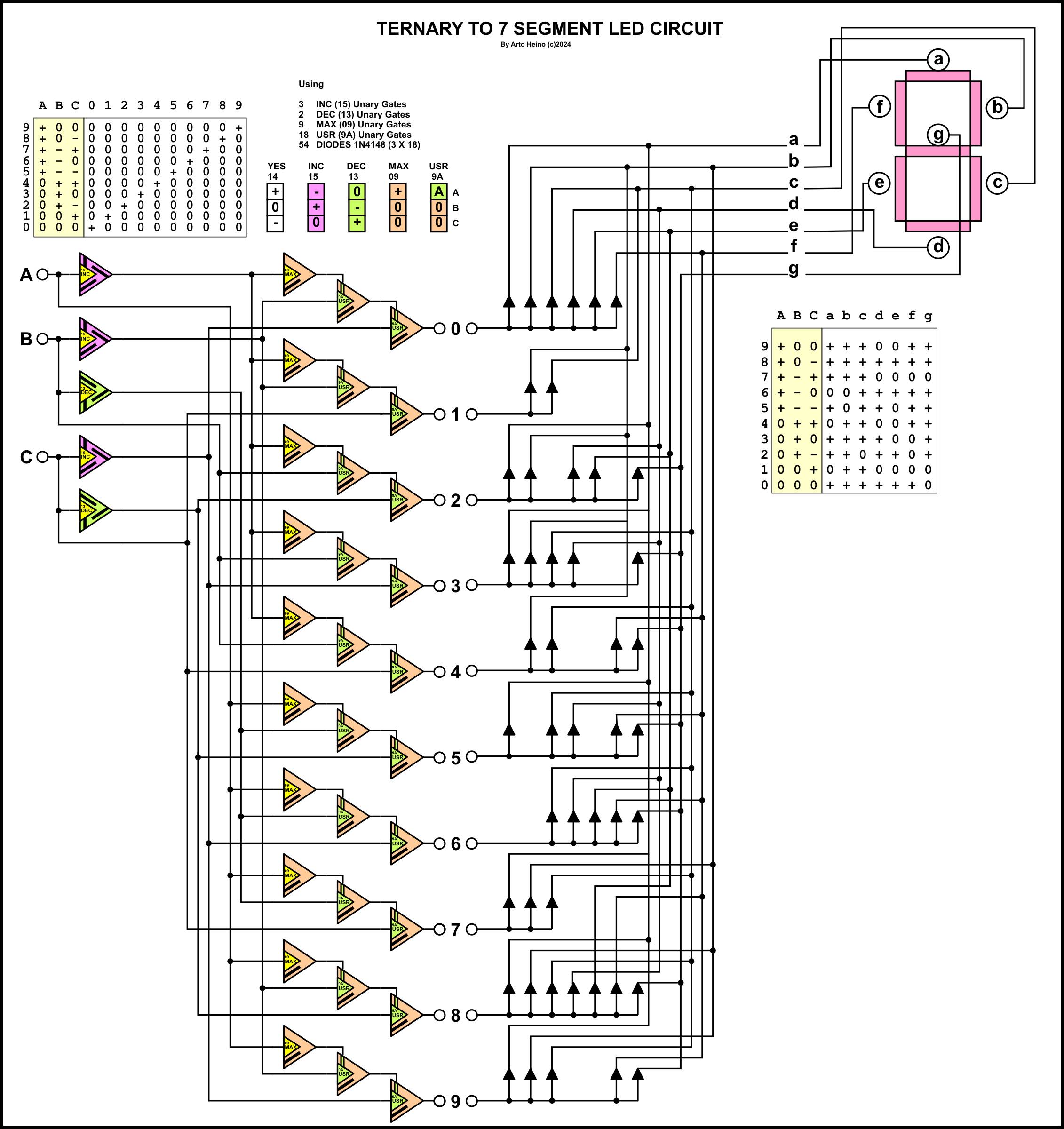
7 Segment Circuit
The final section is the Ternary to 7 Segment circuit. The first circuit (2A) is a basic 0 to 9 Led from a 3 Trit input, using the 3 Unary Gate logic from my earlier design (1C), the second circuit (2B) gives you another 9 more selections. Ternary easily uses negative numbers to increase data width selection, more elaborate schemes could be accomplished, like a complete 27 symbol choice, if I used all 13 positive numbers and all 13 negative numbers and zero.
2A
2B
Both of these designs use Diodes to accomplish the 7 Segment interface, making it suitable for a LED chip such as a Common Cathode TOS5121AR (Titan), LSD505400 (PlusOPTO), LTS-5003AWC (LITEON). You could even make your own with Leds or use a Large display.
I hope to finish my Division section of my Ternary ALU very soon, so far I have Addition, Subtraction, Multiply and a few Logic gates. I am still designing the shift registers and memory, while the ROM will be programmable with switches, I am basing it on 81 Trits at present.
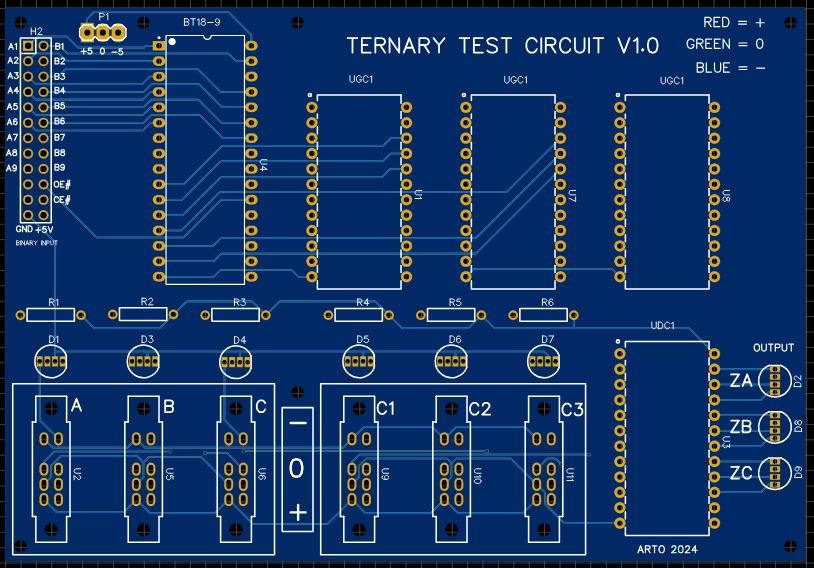
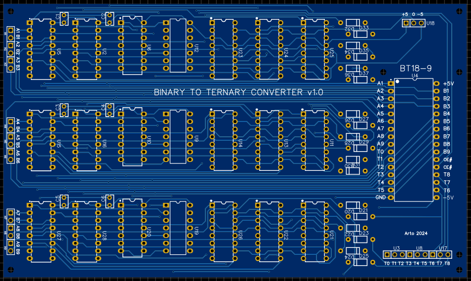
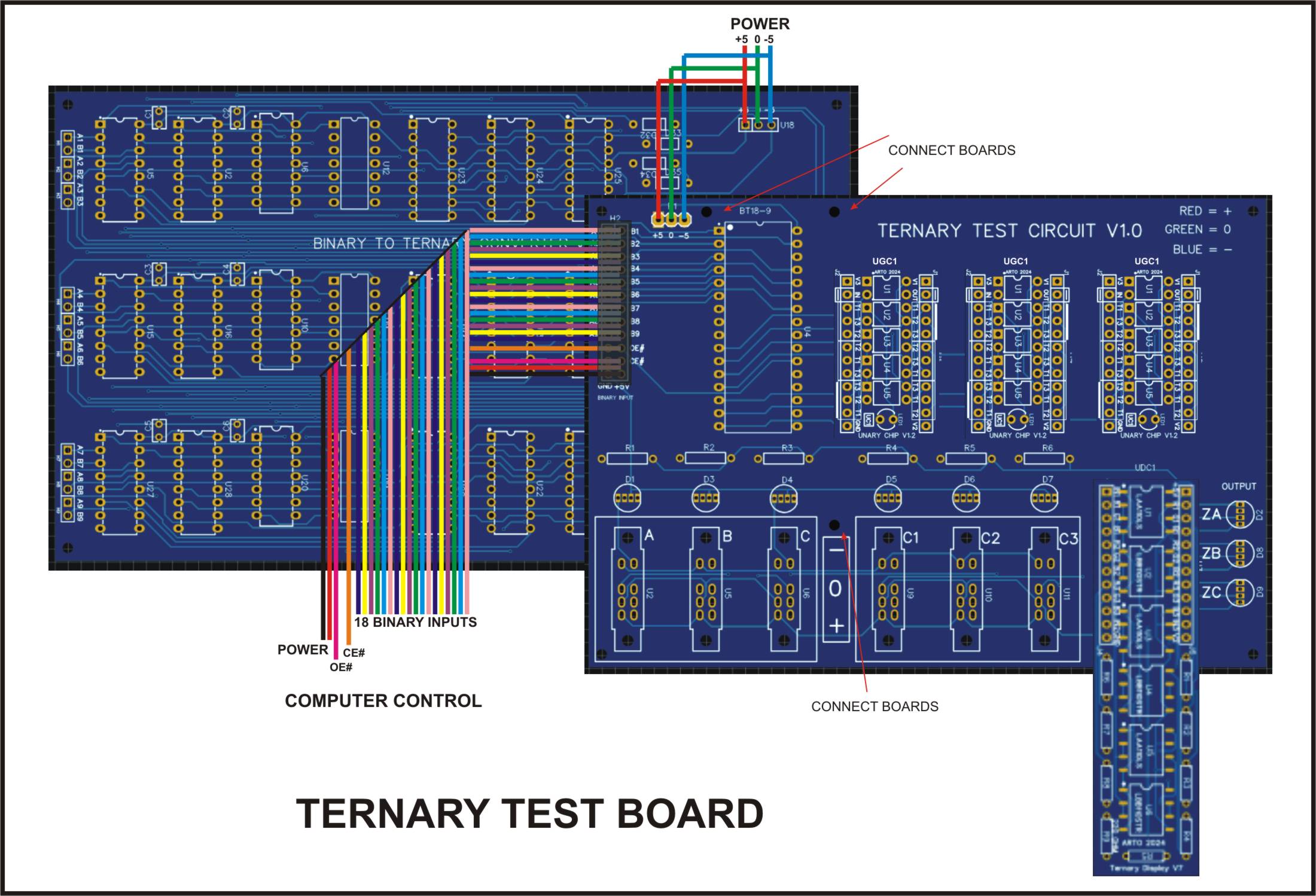
This board can accommodate 3 ternary chips the “BT18-9”, “UGC1” and “UDC1”, all of which are separate units, the BT18-9 needs either a set of ribbon cables with a socket or it can be directly connected with some HDR pins such as the connection diagram into the test board.
BT18-9
18 Binary paired Inputs (A1 B1) to (A9 B9) 9 Ternary outputs T0 to T8 OE# = output enable (you can set inputs then set to 0) CE# = chip enable (you must enable to 0 to start chip) +5V GND -5V
UGC1
1 Ternary input 1 Ternary output 1 led indictor of (-) 6 sets of programable inputs, in order
T1 T2 T3 T2 T3 T1 T3 T1 T2
T1 T3 T2 T2 T1 T3 T3 T3 T1
You can only connect 1 set at any one time, if you use a set of 3 jumper pins on all of the sets you could swap your combinations. These combinations will change your inputs into any one of six possibilities. This could also be done by using a analogue chip in a separate circuit.
UDC1
3 Ternary inputs 3 sets of 3 colour led outputs 3 sets of 3 colour led outputs (mirror of 1st set) So you could use these as Binary output switches or sensors as required. GND V1 = +5V V2 = spare 1 (-5v)
There are 3 ternary input switches (A B C) for all three RGB outputs (ZA ZB ZC) to function, there are also 3 selectors that need to be programmed first. Two of these are programmable by a binary source, while the other is by the onboard switches (C1 C2 C3). The current footprint of the display chip is 24pin pdip, even though the board is longer. As this is still only version 7, more work to do yet and I will eventually make it fit inside the boundary similar to the UGC1 board, on version 8 or 9. I am using optical relays in this design, something that I found useful in my ternary work.
Starting from a Binary input where you have 2 bits to make a ternary trit:
00 = + 10 = 0 01 = –
The bit combination “11” is not valid and will not be used even though it is available as a binary output. The ternary converter ignores it.
Here are the 27 Unary gate combinations that are available and the binary combinations that will create them all. The UGI is the “Unary Gate Index”, numbering of all the gates in a system I have shown on my previous blogs.
Starting with the A1 and B1 as the first pair, then the A2,B2 then A3,B3, these three sets will give you a Unary set of 3 that will configure the basic Unary Chip “UGC1” to one of the 27 gates.
The second set A4,B4 + A5,B5 + A6,B6 will configure the next UGC1 gate. The third set are the switches C1,C2,C3 these will give you another UGC1 gate for you to use.
The outputs ZA,ZB,ZC correspond to the input data A,B,C, where your programmed UGC1 gate is being used to compute your result into the Z Led outputs. Where:
Red = + Green = 0 Blue = –
The input switches A,B,C,C1,C2,C3 also have RGB LEDs.
I hope this might start your interest in Ternary Logic and Computation, regards Arto.
** I have added UDC1 V8 to the Zipfile **
Ternary Test Boards PCB1D Zipfile
Al the PCB and Schematics for this project.
EasyEDA files only.
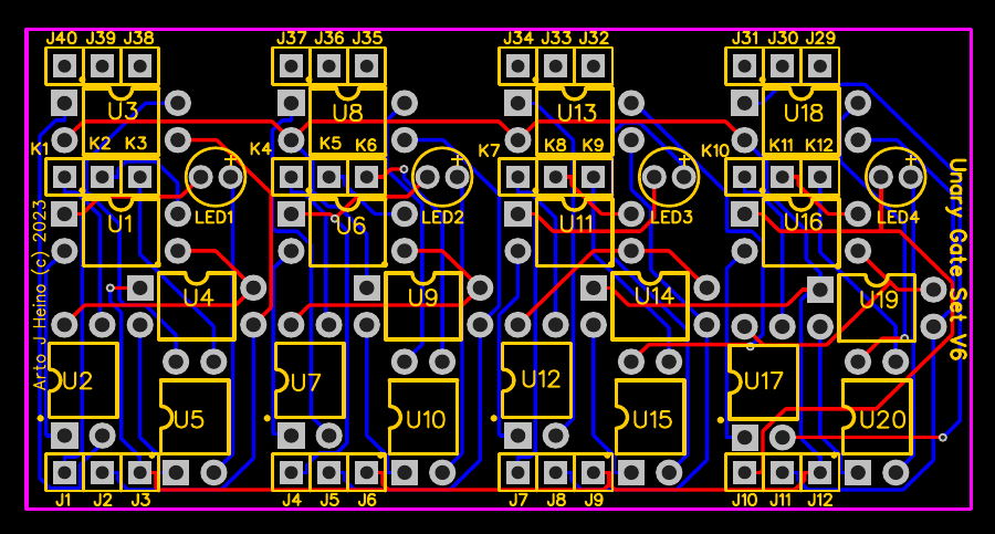
To start the journey of discovery, we must have all the building blocks and tools ready to use as creativity requires a selective group of useful mechanisms to achieve a modicum of feed back to keep the momentum going forward towards interesting and useful discoveries. The Ternary building block are here, along with a Binary controller that you can use to design your Logic elements as needed. I have shown previous Unary gates and they are still usable in these designs. I decided to put 4 gates in one unit so wiring can be simplified when you create the 2/3/4 input gates. For a 2 input gate you need 3 gates for the columns and a summing gate and 3 gates for the rows a summing gate for the rows and the result. This makes it simpler, you will only need 2 unary boards for an 2 input gate, a base board was designed to make this easier, these can be stacked, as high as required.
Parts List for each Unary Gate V6
U1,U3,U4 _________G3VM-353A U2,U5 ____________G3VM-61A1 U6,U8,U9 _________G3VM-353A U7,U10 ___________G3VM-61A1 U11,U13,U14 ______G3VM-353A U8,U15 ___________G3VM-61A1 U16,U18,U19 ______G3VM-353A U17,U20 __________G3VM-61A1 LED1,2,3,4 ________3mm Blue 36 x ______________Male/Female headers 20 x ______________4 Pin sockets (if required) 1 x _______________Unary Board V6
Parts List for Base Boards
4 x _______________24Pin Fmale Header 8 x _______________3 Pin
Parts List for Binary to Ternary Gate Selector Board
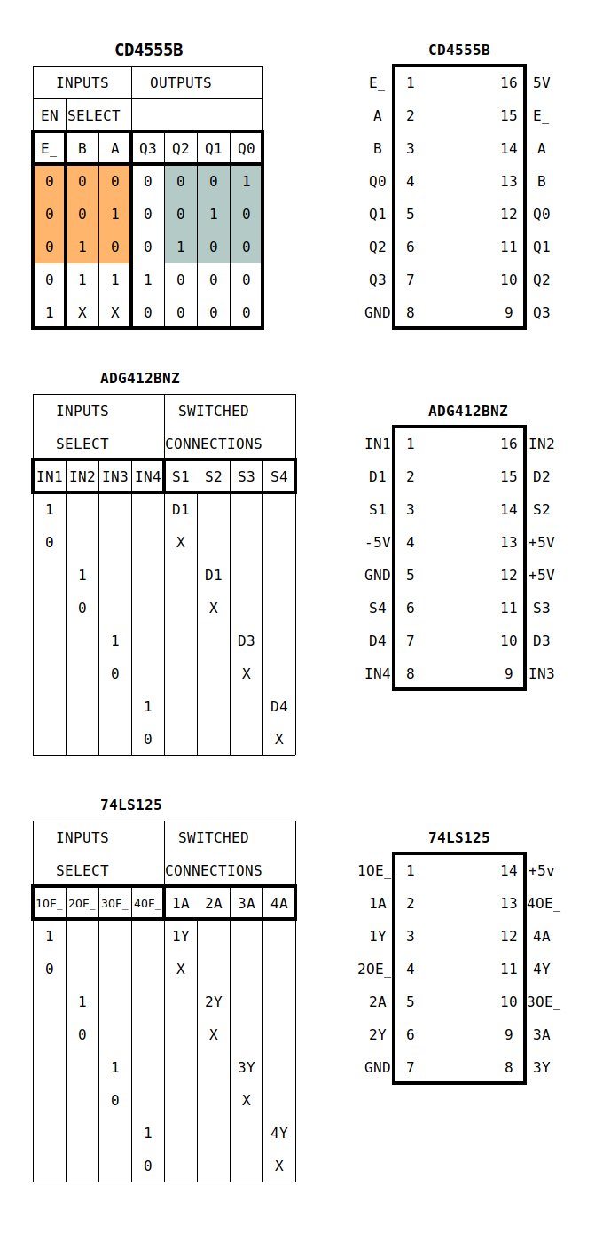
6 x _______________CD4555BE 9 x _______________ADG412BNZ C1,C2,C3,C4,C5,C6 _100 nF Caps D1-D12 ___________1N4007 D19,D20,D21,D22 __1N4007 1 x _______________LM7805 1 x _______________LM7905 C7,C10,C12,C22 ___47uF Electrolytic Caps Led1 _____________Led R1 _______________1K 3 x _______________6 Pin 3 x _______________5 Pin 15 x ______________8 Pin Dip 1 x _______________7 Pin Dip 1 x _______________74LS125
1 x _______________LAA110LS 1 x _______________LBB110STR 3 x _______________220 Ohm 3 x _______________1xPin hdrs 2.54 1 x _______________4 pin hdr 1.27 1 x _______________RGB PCB board
Parts List for TMS9995 Board
1 x ________U8 ____74LS138 1 x ________U5 ____74LS32 1 x ________U6 ____MAX232CPE 1 x ________U7 ____TMS9902 1 x _____U11+U12__TMS9901 x2 1 x ________U1 ____TMS9995 1 x ________U4 ____74LS04 1 x ________U3 ____62256-07 SRAM 1 x ________U2 ____M27C256 EPROM + Binary Data Cortex + Terminal 1 x _______________DB9 RS232 RA port 1 x _______________Header 6 Pin C1-C8 ____________100nF C11,C12___________100nF C16 -C20 __________1uF Electrolyticn R1________________10K R2 – R6____________1K C13, C14 __________15pF X1 _______________12 Mhz XTAL 1 x _______________LED21 LED indicator 1 x _______________SW4 Micro switch C15 ______________10nF 4 x _______________10 pin RA Male Pin Headers 1 x ________U9 ____LM7805 C22, C23 __________47Uf DC1 ______________9v input Jack 3 x________________40 Pin Dip 2 x _______________ 28 Pin Dip 2 x _______________ 14 Pin Dip 2 x _______________ 16 Pin Dip 1 x _______________ 18 Pin Dip 1 x _______________TMS9995 SBC PCB Board (Conner Stuarts Design)
Boards
Unary Gate Base Board V6 Unary Gate Base Board Singles V6 Binary to Ternary Gate Controller V1 Ternary Input Switches Ternary Bit Display TMS9995 SBC
Each Unary board consists of 4 separate Unary Gates they can be used as a set or individually, depending which base board you use.
The Unary Gate Base Board has been configured as a 2 input gate A, B and the result in C.
The Unary Gate Base Board Singles is configured to use as either a 2 input gate by wiring it as required or as single chains or groups.
J1, J4, J7, J10 are your ternary inputs, while J2, J5, J8, J11 are your outputs to each gate.
K1, K2, K3 are configurable with J40, J39, J38 as a matrix to give you all 27 Unary configurations. The interconnections are configurable with a small 6 pin cross connected board, or you can use jumper cables if you choose.
Controller Board
This has a 12vac input and 18+3 pin binary input and a 3 pin ternary output. It was designed to connect to a TMS9995 SBC with CRU outputs and have software to control the gate configuration in hardware.
With Five Boards there are 45 binary controls which will give you a Ternary Multiplexer made of five 2 input gates and 3 Unary gates. Once you have tested and configured your logic, then you can use the base board with plugin matrix connectors as your final gate design.
Setting Your Bits
H1, H2 and H3 are your binary control bits to select each gate type. You select 6 bits to as either decimal or Hex to each unary port. I added U28(74LS125) and U29 3 pin header which is used to switch each gate on, under software control as required.
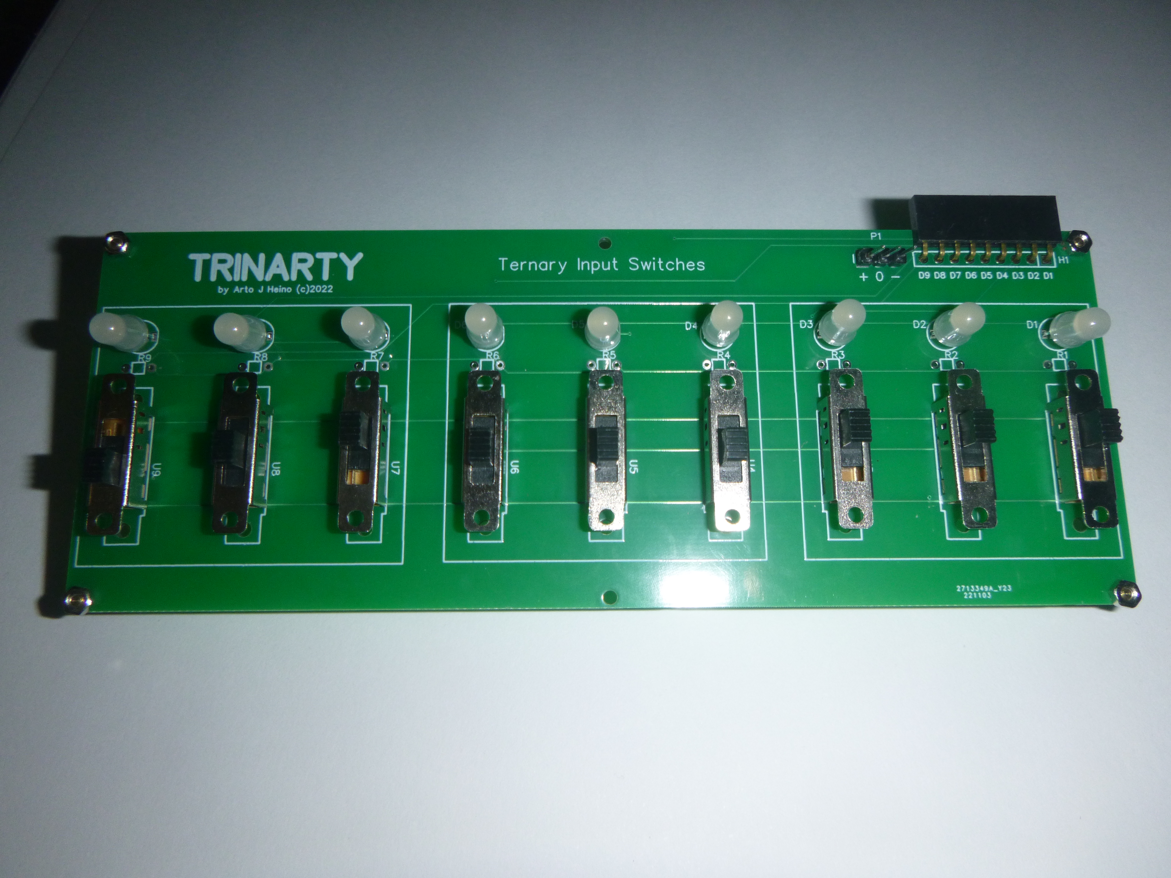
Ternary Input Switches
This board has 9 ternary outputs and can be used to control the A+B inputs on the Unary boards. There is 9 RGB indicators for the slide switches, Red = +5v , Green = 0v , Blue = -5v.
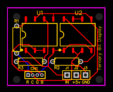
Ternary Bit Display
This small board gives you a visual indication of your output bits, Red = +5v , Green = 0v , Blue = -5v
Listed below is the Program to control the Ternary Gate Selector. If you want to attach more Selector boards you will need to expand the CRU outputs. I have left the header J5 to allow CE for more TMS9901 to be added at some point. The next version will also have have mounting board for 4 more chips, giving a total of 96 outputs.
Where 21 are needed for each 2 input gate, this allows control of 4 2 input gates, 84 pins , leaving you 12 spare pins for other controls.
This is a Cortex Basic program to control one two input gate.
8 REM TERNARY GATE CONTROL 9 REM *** BY ARTO HEINO 2023 ** 10 REM OUTPUT ON 9901 PORT BIT 0 to bit 20 (21 BITS) 11 REM TO CONTROL TERNARY 18 BIT GATES + 3 BIT CONTROL 12 REM 13 REM SETUP BASE ADDRESS OF 9901 to 64 decimal = >0040 HEX 14 BASE 64 15 DIM TR(27,6) 17 REM DISABLE EACH CD4555BE CHIP 18 CRB(16+18)=0 19 CRB(16+19)=0 20 CRB(16+20)=0 24 REM LOAD 27 TERNARY GATE BIT DATA 25 RESTORE 27 FOR Z=1 TO 27 28 FOR X = 1 TO 6 29 READ TR(Z,X) 30 NEXT X 31 NEXT Z 32 REM SELECT 3 GATES 33 FOR A=1 TO 3 36 PRINT “COLUMN “; A 38 PRINT “SELECT GATE 1 TO 27” 39 INPUT GT 40 IF GT<1 OR GT>27 THEN GOTO 38 42 FOR BT=1 T0 6 45 REM SET HIGH OR LOW 48 CRB(15+BT+(A*6-6)) =TR(GT,BT) 56 NEXT BT 57 NEXT A 60 REM ENABLE EACH CD4555BE CHIP 61 CRB(16+18)=1 62 CRB(16+19)=1 63 CRB(16+20)=1 64 END 65 REM DATA FOR GATES 66 REM H1 + H2 + H3 101 DATA 0,0,0,0,0,0 102 DATA 1,0,0,0,0,0 103 DATA 0,1,0,0,0,0 104 DATA 0,0,1,0,0,0 105 DATA 1,0,1,0,0,0 106 DATA 0,1,1,0,0,0 107 DATA 0,0,0,1,0,0 108 DATA 1,0,0,1,0,0 109 DATA 0,1,0,1,0,0 110 DATA 0,0,0,0,1,0 111 DATA 1,0,0,0,1,0 112 DATA 0,1,0,0,1,0 113 DATA 0,0,1,0,1,0 114 DATA 1,0,1,0,1,0 115 DATA 0,1,1,0,1,0 116 DATA 0,0,0,1,1,0 117 DATA 1,0,0,1,1,0 118 DATA 0,1,0,1,1,0 119 DATA 0,0,0,0,0,1 120 DATA 1,0,0,0,0,1 121 DATA 0,1,0,0,0,1 122 DATA 0,0,1,0,0,1 123 DATA 1,0,1,0,0,1 124 DATA 0,1,1,0,0,1 125 DATA 0,0,0,1,0,1 126 DATA 1,0,0,1,0,1 127 DATA 0,1,0,1,0,1
Here is the layout for the SBC and the Ternary Gates.
An alternative design without the SBC and just putting units together.
Here are a few pictures regarding some of the components.
This is the CODE for the 27 selections of Unary gates, H1,H2,H3 CRU outputs.
Here are the PCB’s for the Basic boards.
If you want to see more of this type of content, I would appreciate your support to help pay for more original designs and parts. I hope you enjoy this work, regards Arto.
Ternary PCB1A Zipfile
All the PCB and Schematics for this project. EasyEDA files only.
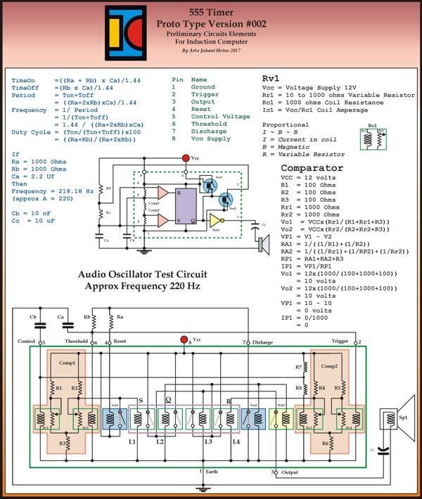
I am back from the wilderness, the experiences of Spring has overwhelmed my Audio and Visual organs, natures beauty is beyond any simple description. The last post I never mentioned the Trinary system that took my designs closer to a complete new type of thinking to develop a Trinary ALU, much more interesting than the Binary approach. Here is the 555 timer I promised from the last post, it is closer to a build-able relay design than my first prototype.
I didn’t show any parameters for the Basic Logic Cell. Here is my sizes and reasoning:
The Basic Logic Cell – Logical Unit
Working from the true measure the Royal Cubit approx 523.24mm, rounding to 525mm. The Palm is four fingers and seven palms make the Royal Cubit.
75mm x 75mm Sqr (aprox 3″ x 3 “)= 1 square Palm.
18.75mm Thick(rounding to 19mm, aprox 3/4” ) = 1 finger thick.
This was why I chose the Ancient Royal Cubit, when you measure the longitudinal velocity of light in royal cubits equals exactly 900000000. Thus it is the exact measure of the Royal Cubit.
Velocity of Light = C
= 299792458 mtrs sec
Longitudinal Velocity of Light = Pi/2 x C
= 1.5708 x 299792458
= 470912891.8272 = CL
Therefore
= CL/900000000
=470912891.8272/900000000
= 0.5232365 Mtrs
= 1 Royal Cubit
This means all your measures you use on materials is concordant to a universal standard, so by coordinating Electrical, Sonic and Hydraulic wave forms in your Logical Unit, all the impedance issues would be known, thus engineer-able.
The Universal Binary Engine
To complete my journey back to relays here is one draft of the Universal Binary Engine, it was designed to be used with a rotary commutator in mind, I was considering the technology of 1900 and the implementation of the Tesla tower as a the hub of computing the Longitudinal Ground Wave communication traffic he would have had to encounter if his tower was finished. Here are my preliminary data covering the commutator and/or relay computer. I have dubbed it “The Universal Binary Engine“, it has motoring logic built in, so a rotating system is viable, a whole new way of conveying intelligence through simple matrix connections with commutators , setting up codes for binary transmission in as many bits as needed. This would be similar to the type of computer switching system Tesla could have worked out during his Wardenclyff period, to direct the control of a complex communication system, with subscribers numbering into the hundreds of millions, not bad for pre-transistor or valve era. Each bit would be just another commutator in rows of switching array commutators, this way you can accommodate large address locations on the globe using a whole wave node number(Earth circumference wave number derived from the frequency of operation) and the directions NSEW as your location matrix. I have a vision in my mind regarding the operational frequencies and mechanical rotating frequencies to make such a system operate as a World Wireless System (NOT Radio), here is a draft PDF of one of my ideas. Here. As this was about laying the most simplest wiring and layout, where you could his own switching systems as per Patent 685953, as illustrated in my Volume I, page 343. I always draft my original designs by free hand sketches and hand written work books, while I am design the Trinary version as well this way, I only draw my work on computer long after I have cleared up any mistakes, either physically tested or carefully worked out on spread sheets.
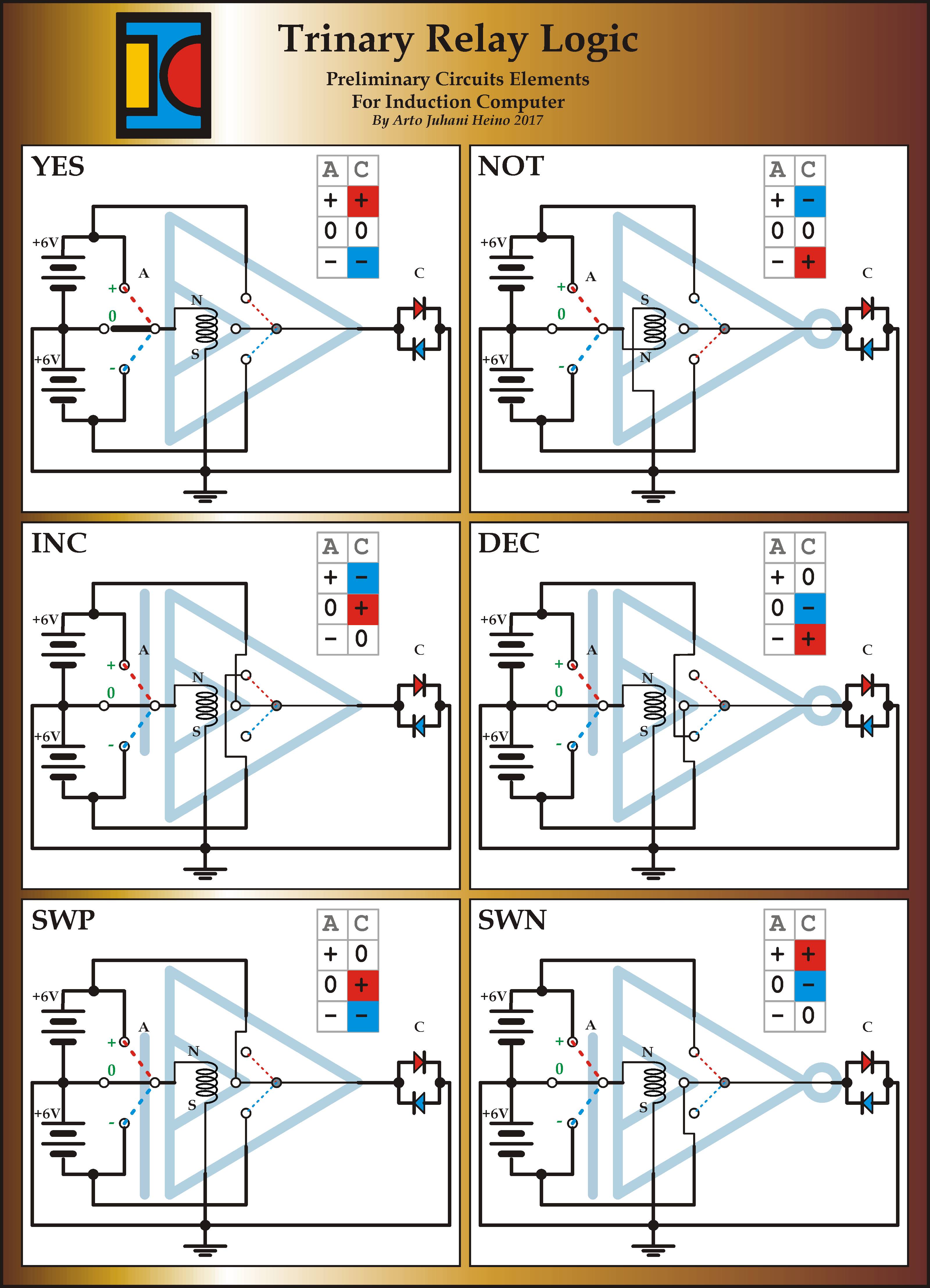
Trinary
Here is list of the first 6 Trinary single input logic gate operations, there are more that I will list shortly.
The Switch is of great importance here, the three distinct actions are of a greater Logic to apply than just on and off. The beginning of a decision tree within the three way action, yes, maybe, no. Where most will see the “0” as a null action it is a vital internal pivot to allow a current flow in be diverted for other operations, as you will see in these basic two input relay gates.
The design scheme was very involved, looking at history and to develop a version that was simple and functional, as my earlier designs show we can still lose the battery and use magnets. The next few gates tested my underlying geometry as a square 5 internal layout.
I have completed the Or, Nor, Xor and Xnor gates and the many other possible logic gates have been noted and configured for future design steps.
The ideas for using the new found parameters available haven’t been explored in the main stream forums as yet, it is not so much the answers they can provide but what are the questions we need to ask and what solutions these gates can provide, we are looking for problems that need solving, this is what will propel these ideas forward. Here is the third page of the steps to arrive at a simple Trinary system with only batteries, switches and leds.
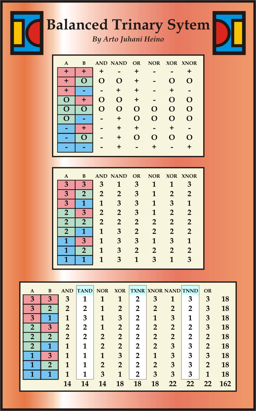
This table below shows some my more interesting breakdown of Logical Gates and new concepts of interaction with the extra three Logical operators to complete another Axiom to investigate.
(18×18)/2 = 162
162 approximates PHI
Thus in an abstracted manner, I am applying natural arithmetic, with a golden Ratio as its final Sum.
I am still working on these and will add another post soon, Regards Arto.
From my last entry I hinted at a 555 relay emulation, I am not quite their yet, I am getting close though. Here is my current stage I am on at the present moment.
I needed an ALU to start things of, so I started on the Half-Adder as a building block, here is my iterations.
The next step is the Full-Adder and its first few iterations from Logic Gates.
Lastly I have included a simple idea of how some of these could be interpreted in the 3D world, more to come on this aspect in a future blog.
If your response is high enough, I will start a Patreon account and begin building the real thing, regards Arto.
It looks like I am reinventing the wheel, minus valves and transistors, this work might even seem redundant to some of the techno-nerds. I assure you this is a step forward, there has been no time in the last 50 years that all those electronic enthusiasts have been able to simplify and create something without an official corporately designed IC package doing all your brain-work for you, leaving nothing for your own original imagination. I was very excited many years ago when many hobbyists made their own computers from discreet transistors and IC packages, while a few even made some relay ALUs.
While I thought of making my own CPU from relays but resisted, I first needed to create a new architecture that could incorporate an open 256 bit CPU and a Analog CPU in one package, while still accessible enough to be built by hand. This was part of my goal, as the architecture had to be robust, to last 1000 years, the components were to be the built environment and the power to drive it should be available 24/7, sounds like a pipe dream of some mad scientist. I only dare to dream of its reality and decided to rediscover the simplicity and the basic technology to make it plausible. The idea of using stone to contain the complex logical matrix that can be accessed via simple interfaces is the final reality, the many steps to arrive at that outcome might outstrip my lifetime, still I will persist, as I cannot dismiss a vision that is clear and within the realms of possibility.
Enough of my machinations, here are some interesting and practically solved devolutions of known devices from my last posting. Here is a FlipFlop made from two relay NAND gates.
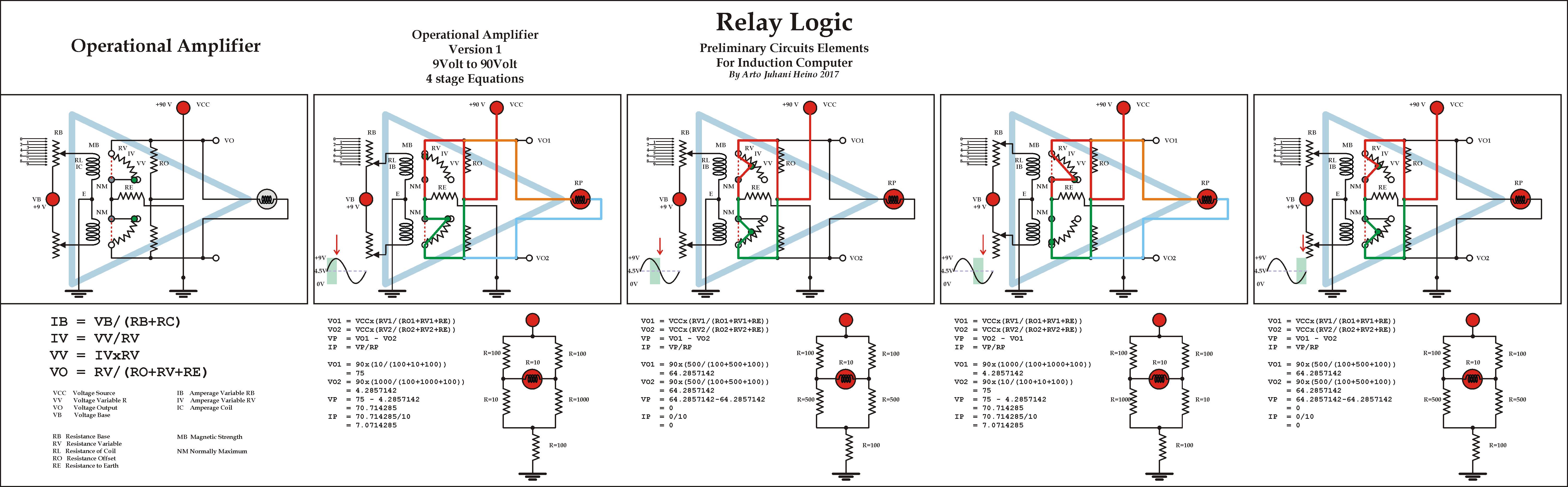
While the idea of a Operational Amplifier kept me awake for a night of two, I hope to emulate a 555 IC chip from my work here, just in time to compete a chapter in my Volume II.
This version should satisfy many of its Integrated Chip operations, still it is a crude and very fundamental design, useful to be expanded upon with a bit more work. I must repeat, I am not an electrical engineer and I have no degree from any University, I am truly a ground up natural scientist, where my tenets of understanding come from a life time of artistic creativity with careful observations and practical applications. I hope those who are interested can learn much from my ideas. Regards Arto.
Here are some interesting combinations using relays as logic gates, which was where I began this first step into the Induction Computer.
As you can see I have “single relays” and “double pole relays” and “Latch relays”, an old technology that goes back to the beginnings of the study of electromagnetism in the 1800’s. My studies into remnant magnetism of different materials, brought me into an understanding of natural rocks and the possibility of using either “Granite”, other rocks or even a poured casting as a magnetically imprinted “Logic Matrix Array”, storing functions, complex procedures, information and even pictures, videos and music.
In the Voltage Multiplier I have even eliminated any semiconductors, even diodes and batteries, while only using coils, capacitors, magnets and relay operations. You can see my process of elimination and the final schematic being without any high tech micro components.
There are a few parts to make the whole system function, here are some of the descriptions for the Voltage Multiplier.
The Slab that must have
1 Remnant Magnetism within permissible limits
2 Flat Surface, possibly engraved for descriptive and functional reasoning
3 Location keys for Imprinter and Reader
The Matrix Imprinter
1 Magnetic Array
2 Electromagnetic Array
3 Reset and Wipe function
The Induction Reader
1 Layered Switch Array
2 Geometric Coil Matrix
3 External Switches/Buttons and Levers/Handles arced or rotary
Physical Actions of Operator
1 Generate Voltage
2 Instigate Switch Operations
3 Discharge to external device
As this blog article is only to describe some of my work, it is not the whole article, that you will find in my next volume of “Talking To The Birds” Volume II. If the interest in these ideas are popular, I would consider a FundMe or Patreon profile and begin the arduous progress of a working system , regards Arto.
Talking to the Birds
Book Available NOW
At Amazon
At Createspace
https://www.createspace.com/4513692
______________________
Cartoons
http://www.scribd.com/doc/106684504/Scraps-Sketches-and-Satire
_______________________
Magic Square
http://www.scribd.com/doc/33050524/The-Magic-Square-of-Three-Crystal


