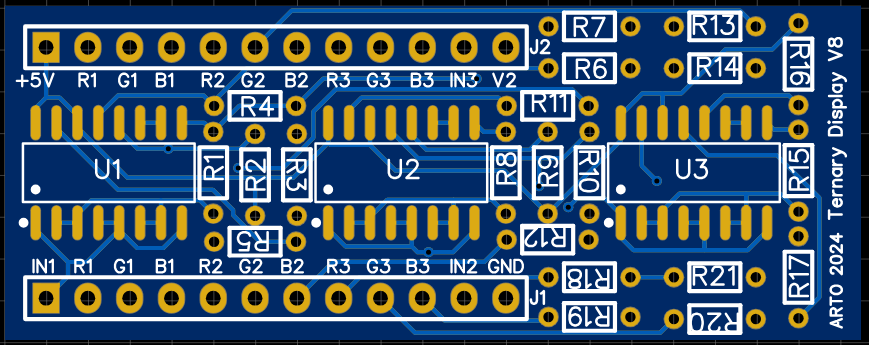
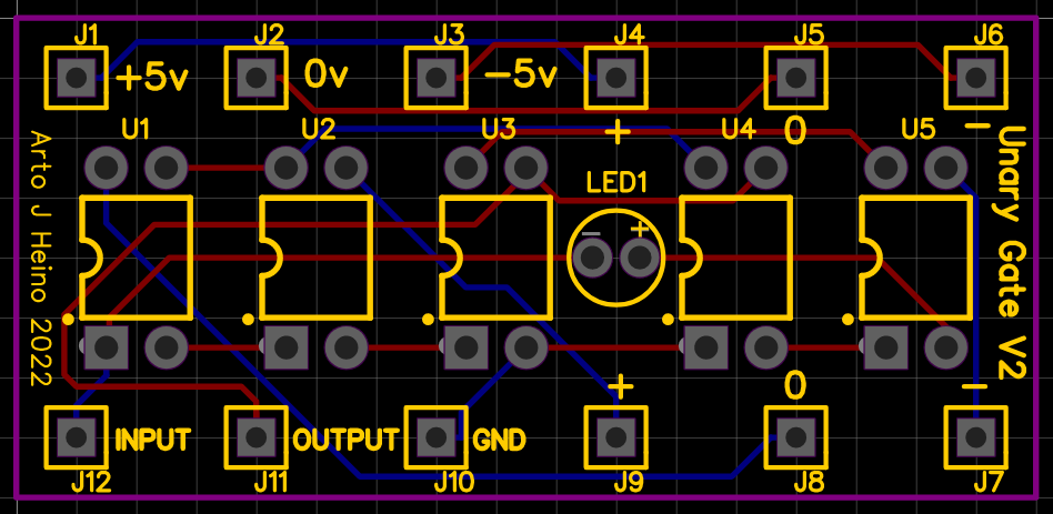
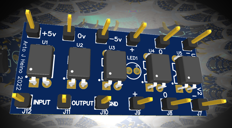
This board design concentrates on the 2 input Ternary Combinations.
I had made many Ternary Gates, here are 2 preferred designs using optical relays, using a 28 pin form.
The display units are less demanding and can be designed in many ways, here are 3 designs, using 24 pins.
The V9 Ternary display unit requires 100 ohm resistors before grounding, if you use V7 or V8 you can just use shorting wires if you requires them, or just leave in the 100 ohm resistors. ( untested)
First of all the 6 switched inputs relates to three 2 input gates which are arranged to give you a maximum of choice.
The first 2 inputs A1 + B1 are directly combined in C1 to create the 2 output gate, designed by the links you combine in 12 pin matrix on the right side of each TNG2-1 chip.
To make your life easier I have put a number of gates that you can use on the bottom of the main board.
The LED outputs are in three groups:
1] switched inputs (6) A1 B1 A2 B2 A3 B3 2] output from each ternary gate (3) C1 C2 C3 3] output from combinations of 3 ternary gates D1 D2 4] output from the last 2 gates E1
To understand the Ternary Gate link matrix, here is a legend:
The jumper settings allows 81 variations, in 3 blocks -1 to 27, 28 to 54, 55 to 81;
I set the basic set up as number 67 from the list above. There are only 36 link combinations that include all three outputs from gates C (they form a top/bottom symmetrical list). Here are the sets:
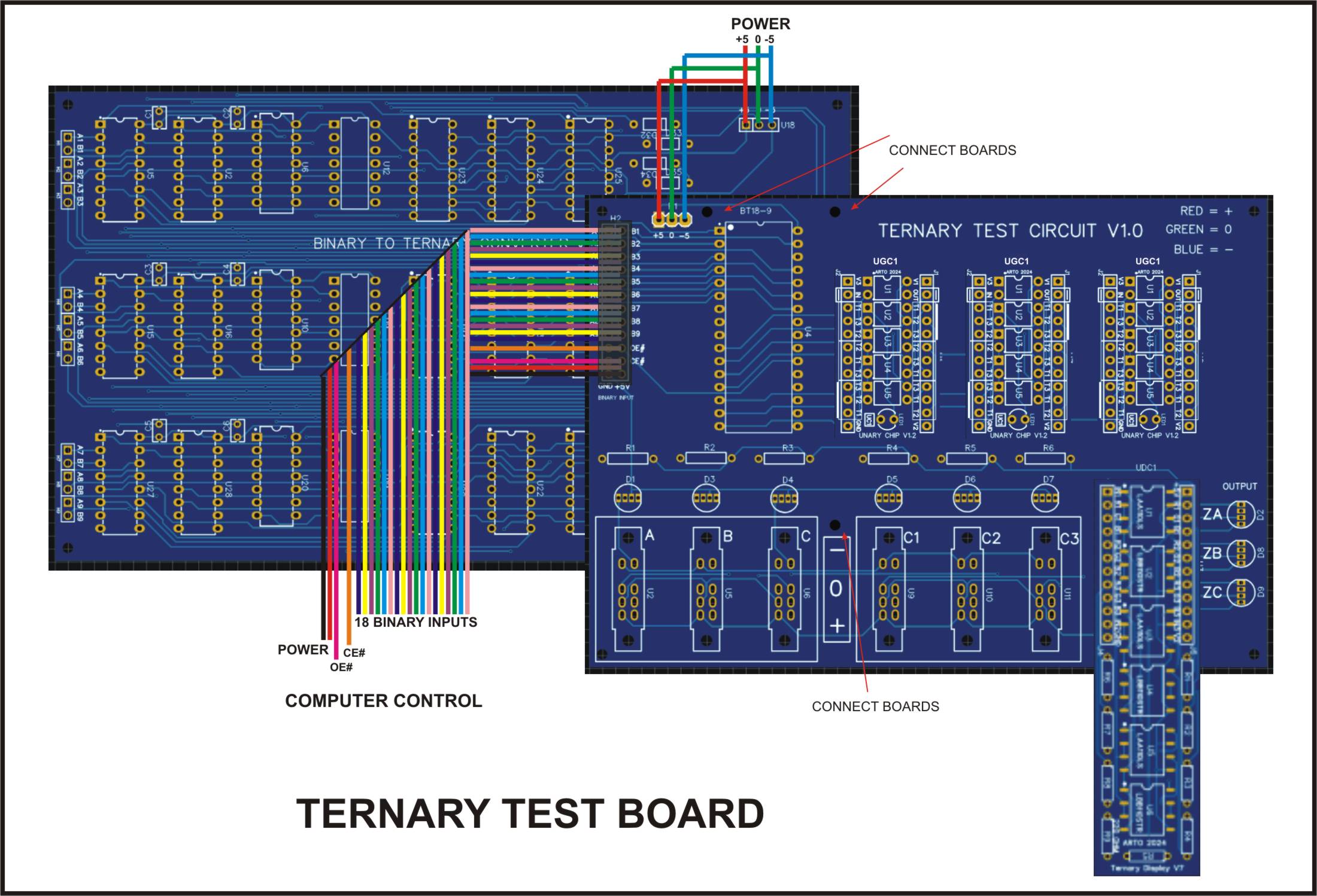
This board can accommodate 3 ternary chips the “BT18-9”, “UGC1” and “UDC1”, all of which are separate units, the BT18-9 needs either a set of ribbon cables with a socket or it can be directly connected with some HDR pins such as the connection diagram into the test board.
BT18-9
18 Binary paired Inputs (A1 B1) to (A9 B9) 9 Ternary outputs T0 to T8 OE# = output enable (you can set inputs then set to 0) CE# = chip enable (you must enable to 0 to start chip) +5V GND -5V
UGC1
1 Ternary input 1 Ternary output 1 led indictor of (-) 6 sets of programable inputs, in order
T1 T2 T3 T2 T3 T1 T3 T1 T2
T1 T3 T2 T2 T1 T3 T3 T3 T1
You can only connect 1 set at any one time, if you use a set of 3 jumper pins on all of the sets you could swap your combinations. These combinations will change your inputs into any one of six possibilities. This could also be done by using a analogue chip in a separate circuit.
UDC1
3 Ternary inputs 3 sets of 3 colour led outputs 3 sets of 3 colour led outputs (mirror of 1st set) So you could use these as Binary output switches or sensors as required. GND V1 = +5V V2 = spare 1 (-5v)
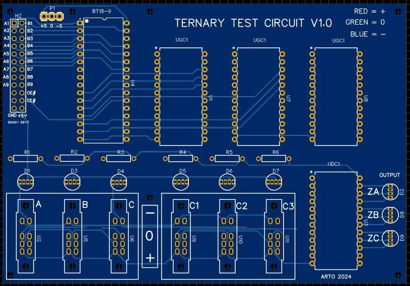
There are 3 ternary input switches (A B C) for all three RGB outputs (ZA ZB ZC) to function, there are also 3 selectors that need to be programmed first. Two of these are programmable by a binary source, while the other is by the onboard switches (C1 C2 C3). The current footprint of the display chip is 24pin pdip, even though the board is longer. As this is still only version 7, more work to do yet and I will eventually make it fit inside the boundary similar to the UGC1 board, on version 8 or 9. I am using optical relays in this design, something that I found useful in my ternary work.
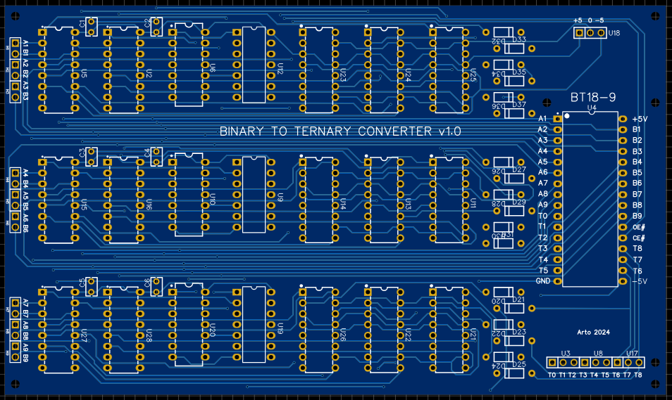
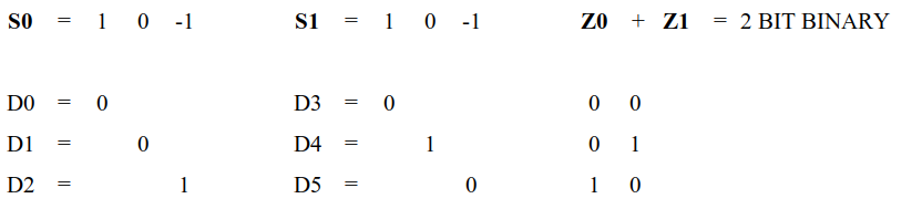
Starting from a Binary input where you have 2 bits to make a ternary trit:
00 = + 10 = 0 01 = –
The bit combination “11” is not valid and will not be used even though it is available as a binary output. The ternary converter ignores it.
Here are the 27 Unary gate combinations that are available and the binary combinations that will create them all. The UGI is the “Unary Gate Index”, numbering of all the gates in a system I have shown on my previous blogs.
Starting with the A1 and B1 as the first pair, then the A2,B2 then A3,B3, these three sets will give you a Unary set of 3 that will configure the basic Unary Chip “UGC1” to one of the 27 gates.
The second set A4,B4 + A5,B5 + A6,B6 will configure the next UGC1 gate. The third set are the switches C1,C2,C3 these will give you another UGC1 gate for you to use.
The outputs ZA,ZB,ZC correspond to the input data A,B,C, where your programmed UGC1 gate is being used to compute your result into the Z Led outputs. Where:
Red = + Green = 0 Blue = –
The input switches A,B,C,C1,C2,C3 also have RGB LEDs.
I hope this might start your interest in Ternary Logic and Computation, regards Arto.
** I have added UDC1 V8 to the Zipfile **
Ternary Test Boards PCB1D Zipfile
Al the PCB and Schematics for this project.
EasyEDA files only.
As a hobbyist I am always trying to work out how certain technologies function, so I decided to look into the PAL, PLA and any programmable logic arrays. So instead of using them as most technicians do I decided to create my own, by standard logic gates and switches, as I am just as interested in the why as the how.
These are my versions of Programmable Logic Arrays based on 74LS chips and 2 position toggle switches. I could try and replicate a standard PAL or PLE chip, but that would just clutter my simple approach as a learning tool. I made them so you can jumper the IC socket into to an existing circuit to test your programming.
LPA-4H10
Using AND/OR arrays, the AND array is either on(throughput) or off(made high) and the OR array is a fixed set to give you the maximum of multiple of outputs (6). My design is based on four 8 input AND gates, which are selectable by 8 switches, giving you a maximum of 32 switches. Using the 4 input bits and it’s inversion to give you 8 internal inputs for each AND gate.
IN1 x IN1# x IN2 x IN2# x IN3 x IN3# x IN4 x IN4# = OUTA1
Your input IN1 to IN4 are you only inputs, all the logic combinations are after your initial input.
AND Gates
2 INPUT, where A=INv and B=INw and Z=OUTAy (v = 1 to 4, w = 1 to 4, y = 1 to 4 )
AND NOT NOT AND AND AFBT ATBF NOR A B Z A# B Z A B# Z A# B# Z --------- --------- --------- --------- 0 0 0 1 0 0 0 1 0 1 1 1 0 1 0 1 1 1 0 0 0 1 0 0 1 0 0 0 0 0 1 1 1 0 1 0 1 1 1 0 1 0 1 0 0 0 0 0
3 INPUT
A B C Z A# B C Z A B# C Z A B C# Z ------------------ 0 0 0 0 0 0 1 0 0 1 0 0 0 1 1 0 1 1 1 1 1 0 0 0 1 0 1 0 1 1 1 1 1 1 0 0 1 1 1 1 1 1 1 1
A B# C# Z A# B# C Z A# B C# Z A# B# C# Z ------------------ 0 1 1 0 1 1 1 1 0 1 0 0 1 1 1 1 0 0 1 0 1 1 1 1 0 0 0 0 1 1 1 1 1 1 0 0 1 0 1 0 1 0 0 0
The abbreviations AFBT and ATBF was devised by me to simplify some of the less known logic gates that are available to the binary combinations. All these odd types of gates can be created with AND, OR, XOR, NOR, XNOR or NAND gates with an inverter on one of the gates as well. I don’t know how useful my ideas are to those Engineers who were educated in Digital Logic, but as an intuitive tool that I have developed, it has given me an insight into applying digital Systems to my Ternary work. As Ternary logic has a massive (19683) number of 2 input elements, your mind boggles at the idea of “Truelean Logic” as opposed to “Boolean Logic” which has only 16 two input elements. Here is the Matrix I developed when I sorted my relay logic elements, it clearly shows how it was developed.
AFBT (AfBt)
Z = (A = False = 0) + (B = True = 1) = True = 1 Z only equals True when (A = False = 0) and (B = true = 1) all the rest are False = 0. If you look at the A input as inverted you will have the same as standard logic, as such:
My Symbol: ____ A ----\ \ | \---------- Z B ----/____|
De Morgans Symbol2 Gated Logic _____ _____ A ----O| \ A ---|>O--| \ | |------- Z = | |--- Z B -----|_____/ B --------|_____/
ATBF (AtBf)
Z = (A = True = 1) + (B = False = 0) = True = 1 Z only equals True when (A = True = 1) and (B = False = 0) all the rest are False = 0. If you look at the B input as inverted you will have the same as standard logic, as such:
My Symbol: _____ A ----\ | | /---------- Z B ----/___/
De Morgans Symbol2 Gated Logic _____ _____ A -----| \ A --------| \ | |------- Z = | |------ Z B ----O|_____/ B ---|>O--|_____/
My Symbolism for multiple inputs
AfBCDEFGt

           *     *     *     *     *     *
Z = (A=0)+(B=1)+(C=1)+(D=1)+(E=1)+(F=1)+(G=1)=1

ACDEFGtBf

     *           *     *     *     *     *
Z = (A=1)+(B=0)+(C=1)+(D=1)+(E=1)+(F=1)+(G=1)=1

ABDFGtCEf

     *     *           *           *     *
Z = (A=1)+(B=1)+(C=0)+(D=1)+(E=0)+(F=1)+(G=1)=1
LPA Logic
The output from the AND array goes into a OR array that is set by 2 inputs using a OR combination, such as:
As you can see there are no more possible combinations than these six for a 2 input OR gate. Another added output is the ANDed output before the ORing which gives you another 4 outputs to use, giving you a total of 10 outputs.
Example 1a:
Here are the equations you can use, by using only IN1 and IN2 as your inputs:
So if you use two inputs, also using only 2 switchs F1 ans F2 of both inputs. Thus you get:
“#” = inversion
“^” = high = 1 (off)
OUTR1 = ((IN1 x F1) x (IN1# x F2^)) + ((IN2 x F1^) x (IN2# x F2))
When a switch “F” is on, then it equals the “IN” input. If “F” if off the it is high (=1).
If, IN1 = 1/0 and F1 is on and F2 is off (1), the rest of the switches are off (1) IN1(F3-F8). Every even switch uses the inverted version of the odd input going to the internal OR inputs.
also, IN2 = 1/0 and F1 is off (1) and F1 is on, the rest of the switches will be off (1) IN2(F3-F8)
IN1(F2) IN2(F1) = switch to high
             AND				OR
             _____
IN1 -0101---|  F1 \  	0101	             ______
            |      |------- OUTA1 ---0101 ---\      \
IN1 -0101--O|__F2_/ 	1111	              |      \
                                              |       \__OUTR1_1101
             _____		              |       /
IN2 -0110---|  F1 \  	1111	              |      /
            |      |------- OUTA2 ---1001 ---/______/
IN2 -0110--O|__F2_/ 	1001
This will give you output to the OUTR1 line, the OUTA1 and OUTA2. This is the output when you swutch IN1(F2) and IN2(F1) to high;
If IN1 = 0 and IN2 = 0 then OUTR1 = 1 , OUTA1 = 0 , OUTA2 = 1 If IN1 = 1 and IN2 = 0 then OUTR1 = 1 , OUTA1 = 1 , OUTA2 = 1 If IN1 = 0 and IN2 = 1 then OUTR1 = 0 , OUTA1 = 0 , OUTA2 = 0 If IN1 = 1 and IN2 = 1 then OUTR1 = 1 , OUTA1 = 1 , OUTA2 = 0
Where switch position “on” allows your input to go through the circuit, while “off” is only “high” (1) so the AND gate now is one less than your total maximum of 8. So if you switch all 8 to “off” this input will be only be a “1”, giving you a “1” on the input to one of the set OR matrix inputs.
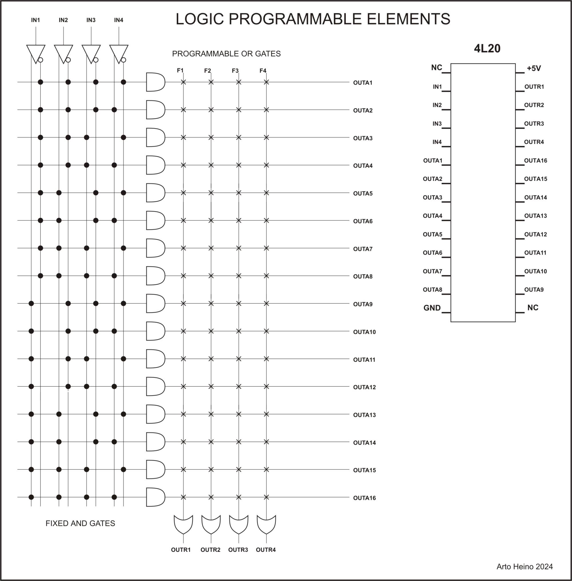
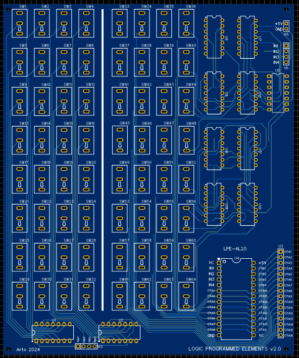
LPE-4L20
You get 4 inputs plus its internal inversions giving you 4 outputs (ORed) and 16 AND combinations. The off switch position is low, thus negating it throughput.
X = input o = inverted input
My first AND Matrix;
1 2 3 4 5 6 7 8 9 1 1 1 1 1 1 1
                  0 1 2 3 4 5 6
x x x x . x x . x . . x . . . .
. . . . o . . o . o o . o o o o

x x x . x x . . . x x . x . . .
. . . o . . o o o . . o . o o o

x x . x x . . x x . x . . x . .
. . o . . o o . . o . o o . o o

x . x x x . x x . x . . . . x .
. o . . . o . . o . o o o o . o
I was going to use this internal format, until I decided to use the standard PLE arrangement.
--------------------------------
   |   |   |   |   |   |   |
1 2 3 4 5 6 7 8 9 1 1 1 1 1 1 1		Net     AND Inverter output
                  0 1 2 3 4 5 6
. . . . . . . . x x x x x x x x   	H1  	A   1A
o o o o o o o o . . . . . . . .		U5_2	    1Y

. . . . x x x x . . . . x x x x 	H2	B   2A
o o o o . . . . o o o o . . . .		U5_4	    2Y

. . x x . . x x . . x x . . x x 	H3	C   3A
o o . . o o . . o o . . o o . .		U5_6	    3Y

. x . x . x . x . x . x . x . x		H4	D   4A
o . o . o . o . o . o . o . o .		U5_8	    4Y
So if you want to implement a 4 input XOR gate:
FnXOR = XOR (IN1 IN1# IN2 IN2# IN3 IN3# IN4 IN4#)
 =
(IN1 X IN2# X IN3# X IN4#) +
(IN1# X IN2 X IN3# X IN4#) +
(IN1# X IN2# X IN3 X IN4#) +
(IN1# X IN2# X IN3# X IN4) +
(IN1 X IN2 X IN3 X IN4#) +
(IN1 X IN2 X IN3# X IN4) +
(IN1 X IN2# X IN3 X IN4) +
(IN1# X IN2 X IN3 X IN4)
Switches used: (from 1 to 64) 5 9 17 29 33 45 53 57 – or – first column (1 to 16) 2 3 5 8 9 12 14 15 are ON all other switches are OFF
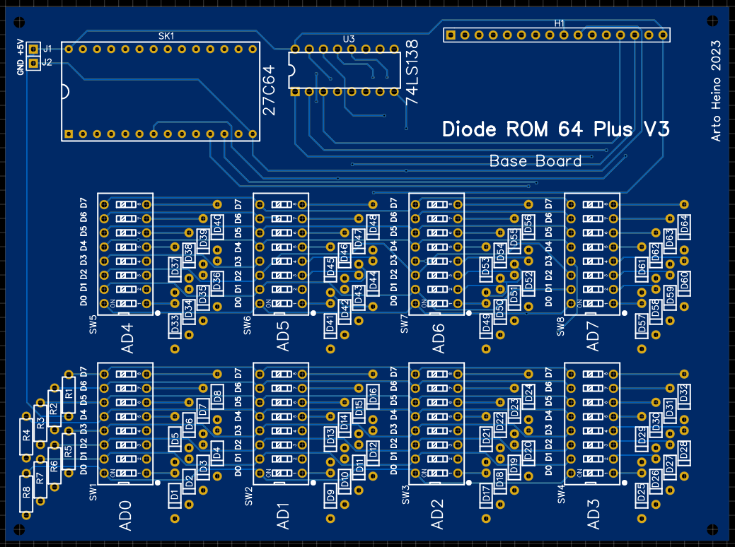
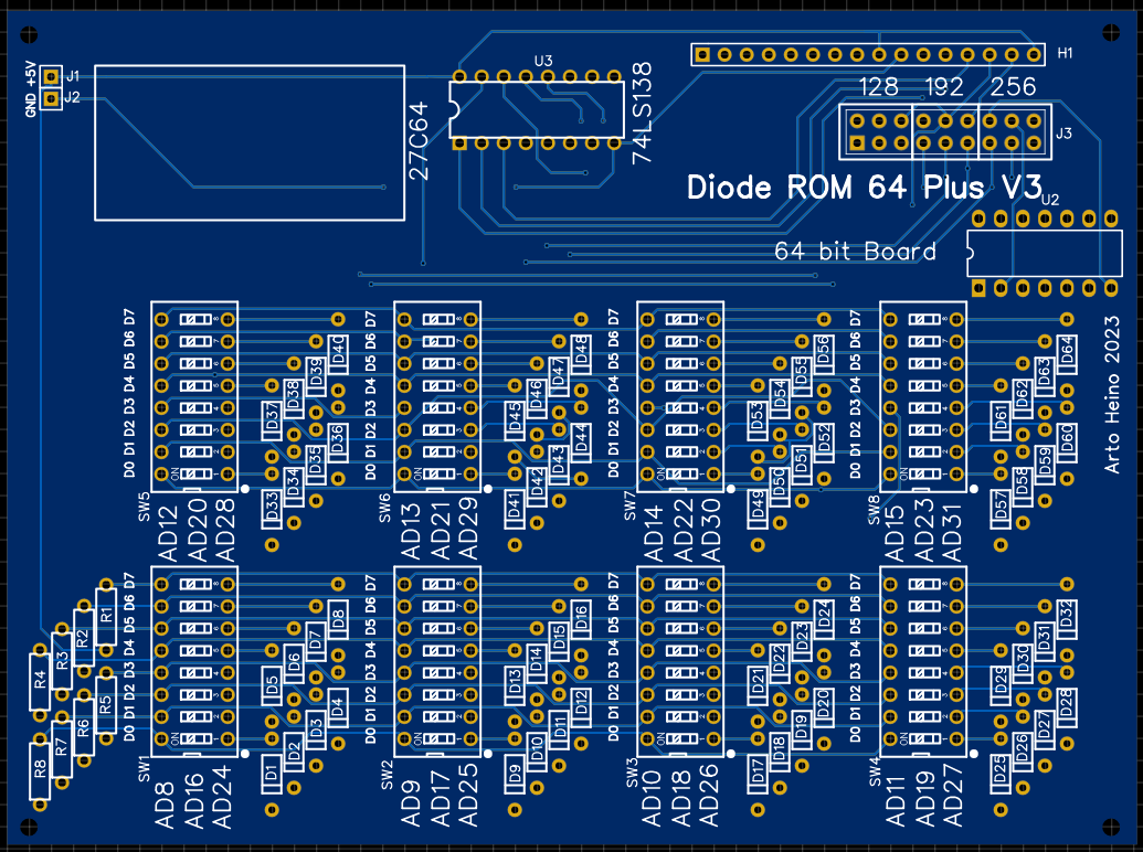
As my research moves along, I decided to create a Diode Memory unit first for binary use, before I implement the ternary memory version. I designed 2 types of boards, the first is the base board which is the first 64 bits or 8 bytes, the 2nd board can be stacked on top to create 128 bits or 16 bytes with more boards on top for 192/256 bits or 24/32 bytes. I will be building these soon, as these designs have not been tested yet, I suggest checking my work, I will confirm these in another blog.
The ROM choice was a 27C64 which is a 8Kx8 and is very popular, available in general stock and I will use it in further designs, the decoder is a 74LS138 which seems to be a great choice for this simple project. The only problem I had was the 138 has only 3 bits to decode, so I had to add a few extra bit of routing to create 32 bytes. The 138 has 3 enable lines GA_, GB_, G1, so the first block I put G1 high and GA_and GB_ would be enabled when both are low, these are from the A3 and A4 lines which are low. The second block I put GA_ low to ground with GB_ and G1 would be A4 as low and A3 as high. As you can see by the diagram I swapped A3 and A4 with GA grounded for the 3rd block, the last block I used an inverter on GB_ from A3 which must be high,
If you are not using 32 bytes then you can ignore the 74LS04 connection. To use each block you must bridge the labelled connectors with jumpers. The Parts list for 2 boards are:
SK1 = 28 pin DIP socket with extended legs
H1 = 16 Pin socket with extended legs x 2
U3 = 74LS138 x 2
R1-R8 = 10K resistors x 2
D1-D64 = 1N4148 Diodes x 2
SW1-SW8 = 8 sw DIP x 2
J1-J2 = Pin for Power x 2
Each corner has 2mm holes , add crews and extended legs as needed x 2
If you choose to build it, you will be limited to 32 bytes. To test the unit you could plug it into to a EPROM reader. My next version should allow up to 256 bytes or more. Regards Arto.
Diode ROM PCB1C Zipfile
All the PCB and Schematics for this project. EasyEDA files only.
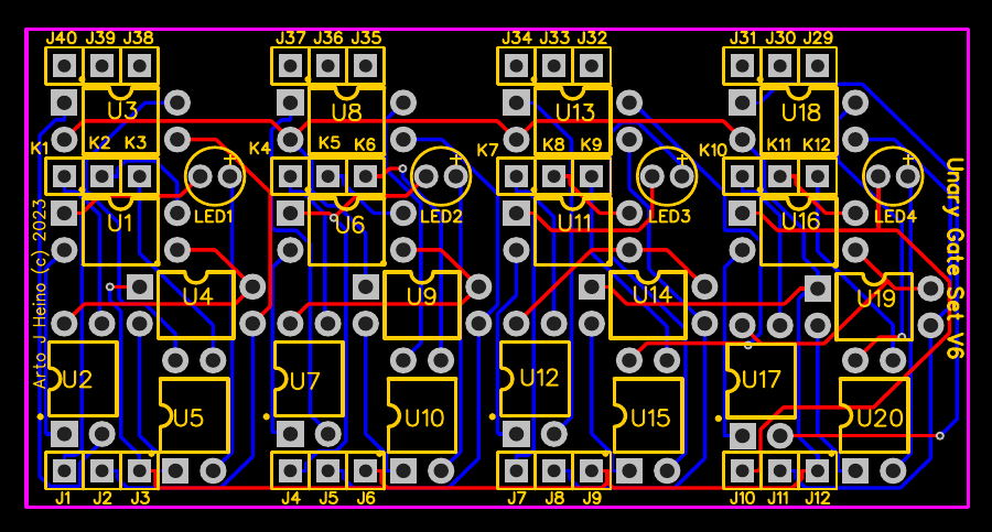
To start the journey of discovery, we must have all the building blocks and tools ready to use as creativity requires a selective group of useful mechanisms to achieve a modicum of feed back to keep the momentum going forward towards interesting and useful discoveries. The Ternary building block are here, along with a Binary controller that you can use to design your Logic elements as needed. I have shown previous Unary gates and they are still usable in these designs. I decided to put 4 gates in one unit so wiring can be simplified when you create the 2/3/4 input gates. For a 2 input gate you need 3 gates for the columns and a summing gate and 3 gates for the rows a summing gate for the rows and the result. This makes it simpler, you will only need 2 unary boards for an 2 input gate, a base board was designed to make this easier, these can be stacked, as high as required.
Parts List for each Unary Gate V6
U1,U3,U4 _________G3VM-353A U2,U5 ____________G3VM-61A1 U6,U8,U9 _________G3VM-353A U7,U10 ___________G3VM-61A1 U11,U13,U14 ______G3VM-353A U8,U15 ___________G3VM-61A1 U16,U18,U19 ______G3VM-353A U17,U20 __________G3VM-61A1 LED1,2,3,4 ________3mm Blue 36 x ______________Male/Female headers 20 x ______________4 Pin sockets (if required) 1 x _______________Unary Board V6
Parts List for Base Boards
4 x _______________24Pin Fmale Header 8 x _______________3 Pin
Parts List for Binary to Ternary Gate Selector Board
6 x _______________CD4555BE 9 x _______________ADG412BNZ C1,C2,C3,C4,C5,C6 _100 nF Caps D1-D12 ___________1N4007 D19,D20,D21,D22 __1N4007 1 x _______________LM7805 1 x _______________LM7905 C7,C10,C12,C22 ___47uF Electrolytic Caps Led1 _____________Led R1 _______________1K 3 x _______________6 Pin 3 x _______________5 Pin 15 x ______________8 Pin Dip 1 x _______________7 Pin Dip 1 x _______________74LS125
1 x _______________LAA110LS 1 x _______________LBB110STR 3 x _______________220 Ohm 3 x _______________1xPin hdrs 2.54 1 x _______________4 pin hdr 1.27 1 x _______________RGB PCB board
Parts List for TMS9995 Board
1 x ________U8 ____74LS138 1 x ________U5 ____74LS32 1 x ________U6 ____MAX232CPE 1 x ________U7 ____TMS9902 1 x _____U11+U12__TMS9901 x2 1 x ________U1 ____TMS9995 1 x ________U4 ____74LS04 1 x ________U3 ____62256-07 SRAM 1 x ________U2 ____M27C256 EPROM + Binary Data Cortex + Terminal 1 x _______________DB9 RS232 RA port 1 x _______________Header 6 Pin C1-C8 ____________100nF C11,C12___________100nF C16 -C20 __________1uF Electrolyticn R1________________10K R2 – R6____________1K C13, C14 __________15pF X1 _______________12 Mhz XTAL 1 x _______________LED21 LED indicator 1 x _______________SW4 Micro switch C15 ______________10nF 4 x _______________10 pin RA Male Pin Headers 1 x ________U9 ____LM7805 C22, C23 __________47Uf DC1 ______________9v input Jack 3 x________________40 Pin Dip 2 x _______________ 28 Pin Dip 2 x _______________ 14 Pin Dip 2 x _______________ 16 Pin Dip 1 x _______________ 18 Pin Dip 1 x _______________TMS9995 SBC PCB Board (Conner Stuarts Design)
Boards
Unary Gate Base Board V6 Unary Gate Base Board Singles V6 Binary to Ternary Gate Controller V1 Ternary Input Switches Ternary Bit Display TMS9995 SBC
Each Unary board consists of 4 separate Unary Gates they can be used as a set or individually, depending which base board you use.
The Unary Gate Base Board has been configured as a 2 input gate A, B and the result in C.
The Unary Gate Base Board Singles is configured to use as either a 2 input gate by wiring it as required or as single chains or groups.
J1, J4, J7, J10 are your ternary inputs, while J2, J5, J8, J11 are your outputs to each gate.
K1, K2, K3 are configurable with J40, J39, J38 as a matrix to give you all 27 Unary configurations. The interconnections are configurable with a small 6 pin cross connected board, or you can use jumper cables if you choose.
Controller Board
This has a 12vac input and 18+3 pin binary input and a 3 pin ternary output. It was designed to connect to a TMS9995 SBC with CRU outputs and have software to control the gate configuration in hardware.
With Five Boards there are 45 binary controls which will give you a Ternary Multiplexer made of five 2 input gates and 3 Unary gates. Once you have tested and configured your logic, then you can use the base board with plugin matrix connectors as your final gate design.
Setting Your Bits
H1, H2 and H3 are your binary control bits to select each gate type. You select 6 bits to as either decimal or Hex to each unary port. I added U28(74LS125) and U29 3 pin header which is used to switch each gate on, under software control as required.
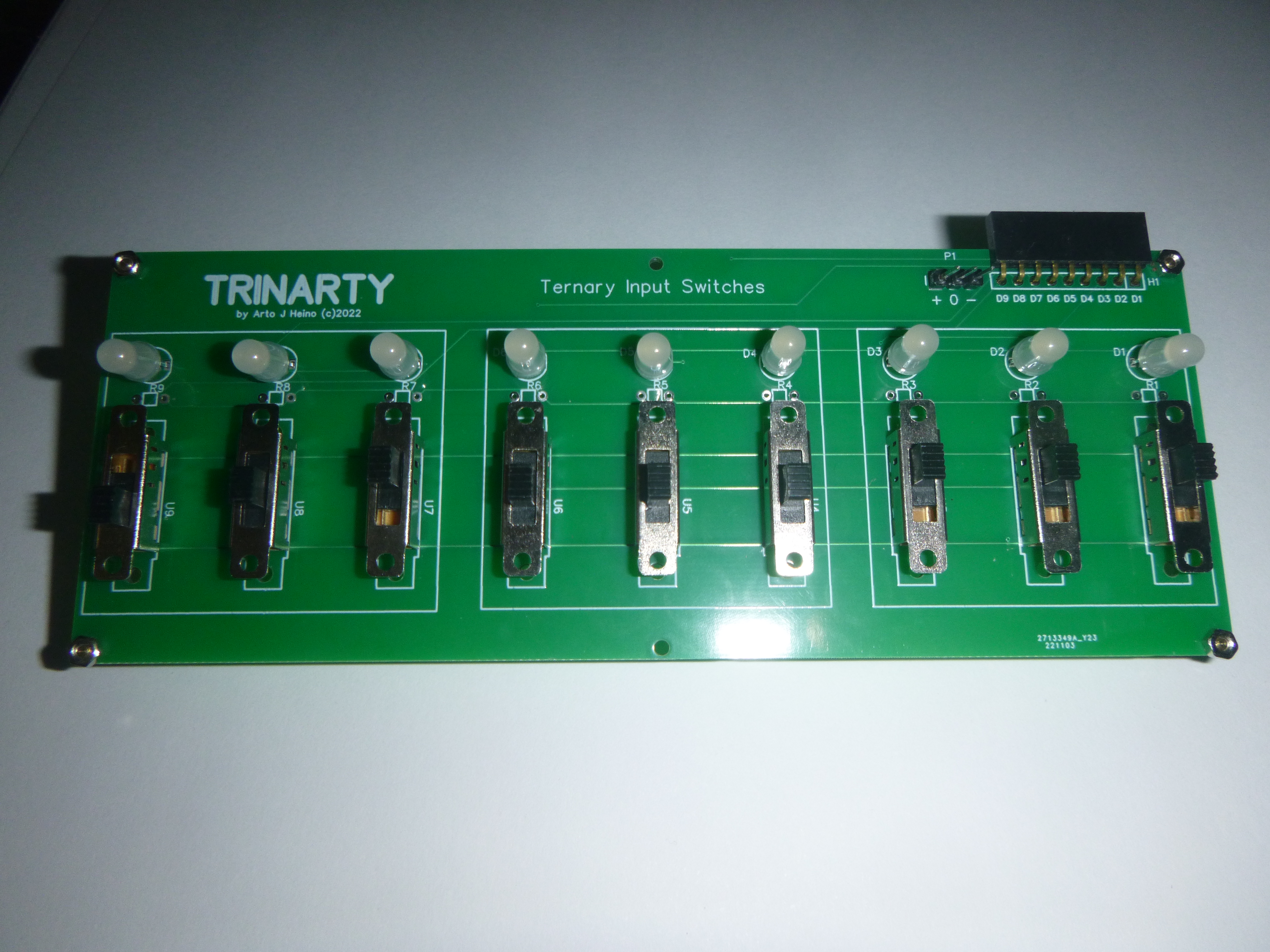
Ternary Input Switches
This board has 9 ternary outputs and can be used to control the A+B inputs on the Unary boards. There is 9 RGB indicators for the slide switches, Red = +5v , Green = 0v , Blue = -5v.
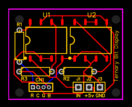
Ternary Bit Display
This small board gives you a visual indication of your output bits, Red = +5v , Green = 0v , Blue = -5v
Listed below is the Program to control the Ternary Gate Selector. If you want to attach more Selector boards you will need to expand the CRU outputs. I have left the header J5 to allow CE for more TMS9901 to be added at some point. The next version will also have have mounting board for 4 more chips, giving a total of 96 outputs.
Where 21 are needed for each 2 input gate, this allows control of 4 2 input gates, 84 pins , leaving you 12 spare pins for other controls.
This is a Cortex Basic program to control one two input gate.
8 REM TERNARY GATE CONTROL 9 REM *** BY ARTO HEINO 2023 ** 10 REM OUTPUT ON 9901 PORT BIT 0 to bit 20 (21 BITS) 11 REM TO CONTROL TERNARY 18 BIT GATES + 3 BIT CONTROL 12 REM 13 REM SETUP BASE ADDRESS OF 9901 to 64 decimal = >0040 HEX 14 BASE 64 15 DIM TR(27,6) 17 REM DISABLE EACH CD4555BE CHIP 18 CRB(16+18)=0 19 CRB(16+19)=0 20 CRB(16+20)=0 24 REM LOAD 27 TERNARY GATE BIT DATA 25 RESTORE 27 FOR Z=1 TO 27 28 FOR X = 1 TO 6 29 READ TR(Z,X) 30 NEXT X 31 NEXT Z 32 REM SELECT 3 GATES 33 FOR A=1 TO 3 36 PRINT “COLUMN “; A 38 PRINT “SELECT GATE 1 TO 27” 39 INPUT GT 40 IF GT<1 OR GT>27 THEN GOTO 38 42 FOR BT=1 T0 6 45 REM SET HIGH OR LOW 48 CRB(15+BT+(A*6-6)) =TR(GT,BT) 56 NEXT BT 57 NEXT A 60 REM ENABLE EACH CD4555BE CHIP 61 CRB(16+18)=1 62 CRB(16+19)=1 63 CRB(16+20)=1 64 END 65 REM DATA FOR GATES 66 REM H1 + H2 + H3 101 DATA 0,0,0,0,0,0 102 DATA 1,0,0,0,0,0 103 DATA 0,1,0,0,0,0 104 DATA 0,0,1,0,0,0 105 DATA 1,0,1,0,0,0 106 DATA 0,1,1,0,0,0 107 DATA 0,0,0,1,0,0 108 DATA 1,0,0,1,0,0 109 DATA 0,1,0,1,0,0 110 DATA 0,0,0,0,1,0 111 DATA 1,0,0,0,1,0 112 DATA 0,1,0,0,1,0 113 DATA 0,0,1,0,1,0 114 DATA 1,0,1,0,1,0 115 DATA 0,1,1,0,1,0 116 DATA 0,0,0,1,1,0 117 DATA 1,0,0,1,1,0 118 DATA 0,1,0,1,1,0 119 DATA 0,0,0,0,0,1 120 DATA 1,0,0,0,0,1 121 DATA 0,1,0,0,0,1 122 DATA 0,0,1,0,0,1 123 DATA 1,0,1,0,0,1 124 DATA 0,1,1,0,0,1 125 DATA 0,0,0,1,0,1 126 DATA 1,0,0,1,0,1 127 DATA 0,1,0,1,0,1
Here is the layout for the SBC and the Ternary Gates.
An alternative design without the SBC and just putting units together.
Here are a few pictures regarding some of the components.
This is the CODE for the 27 selections of Unary gates, H1,H2,H3 CRU outputs.
Here are the PCB’s for the Basic boards.
If you want to see more of this type of content, I would appreciate your support to help pay for more original designs and parts. I hope you enjoy this work, regards Arto.
Ternary PCB1A Zipfile
All the PCB and Schematics for this project. EasyEDA files only.
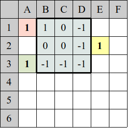
To be clear the multitude of Ternary 2 input gates is a gift to the creative mind, I have written a program that enumerates all 19683 and deemed all of them useful. An example of this is gate 2272 (TAB-index), which is “Tautology” or all “+1”, so any inputs at A and B results in +1 on the output. You might say what is the point of that? Only now it acts like a buffer or a line driver, so it serves a “function” in a ternary circuit or a re-encoder in a more complex circuit. After deciding what is needed to develop a Ternary computer, I first looked to the 27 Unary gates and the all gates that are commonly used in binary circuits, like AND, OR, NAND, NOR etc…which there are a total of 16 and which 6 are deemed the most useful.
Here is the complete set of Binary Relay Logic
Exploring the Trinary logic opens a whole new way of seeing and thinking about computer architecture. For example a multiplexer is a most versatile device when designing circuits so I chose to explore this device to see what can be learnt from applying ternary logic to its internals. In a previous post (https://artoheino.com/2021/05/04/the-2-to-9-decoder/..) I showed my crafted and workable TD2-9 (2 input to 9 output) decoder. this will be the starting point of some new discoveries.
First lets go back to the simplest version the TD1-3 decoder:
I chose this one mainly due to the fact it can be used to decode Ternary to Binary, so one input from a Trinary based system can produce 3 signals to control a Binary based chip. So a mixture of Binary and Trinary is not difficult to attain.
Here is an example of one of my Binary to Ternary Interfaces based on a Analog Devices chip.
I have used a spread sheet to design the small Unary modules and 2 input Ternary Gate modules to develop these designs, they were based on the Ternary Relay designs I have outlined in my previous work.
The spread sheet model has helped me in developing combinatoric circuits and ensure consistent logical flow, as this is a new technological playground and has some crude pointers and intellectual fences to overcome. As the diagram of the 2 circuits show, we can decode with positive or negative numbers without the binary load that is usually a constrictive affair and become overly complex.
After much mind bending Ternary Logic visual calculations and pattern recognition, here is the First Ternary Multiplexer, TM3-1 with a future TM9-2, TM27-3 and TM81-4 as simple extensions. Where as the Binary can only achieve 2-1, 4-2, 8-3 and 16-4, so imagine how versatile these gates can be.
With this TM3-1 you could create a Ternary to binary converter, by using two of these
A Binary to Ternary converter is also possible:
They can also be usable as a 2-2 Encoder in binary:
Also by cascading the TM3-1 you can create the TM9-2.
Choice of Unary Operators
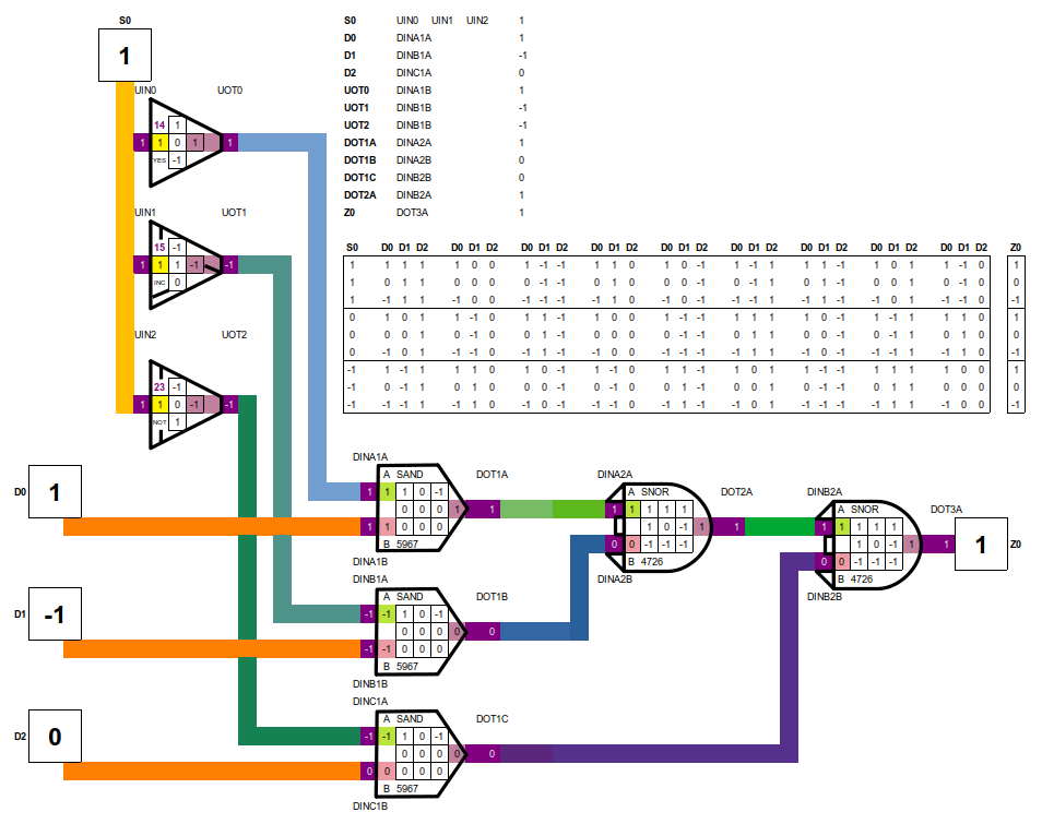
Using the binary combination of AND plus OR gates, I first applied the binary equivalents of the Ternary gates to create the Multiplexer but found the Ternary logic would not cooperate as easily as binary. This is when I realised that the ternary system would have a simpler gate choice to achieve the same result. Instead of TAND I used SAND, which has a simpler matrix, while the DNOR is similar to the TNOR gate. This gave me the start, which later I found that VAND and LAND gates also work.
Ternary 2 input Gates
Ternary Converter
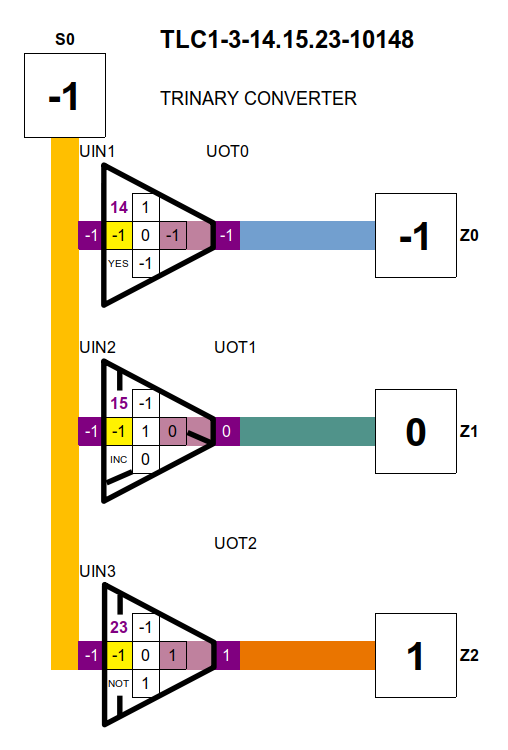
During these discoveries, I realised a ternary converter would be useful by itself. The numbering system describes the 3 gates and the 2 input equivalent.
Example:
TLC1-3-14.14.23-10148 TLC = Ternary Logic Converter 1-3 = 1 input 3 output 13.15.23 = Unary gates used 13, 15 and 23 10148 = The 2 input gate number equivalent 1 to 19686
Hardware Versions
After many attempts to make these circuits simple and easy to follow, I decided to concentrate on the relay versions but started using Photo-MOS Relays instead. This I found to be advantageous as the noise was eliminated and the current consumption decreased with the bonus of high speed. I would like to see a Photo-mos version of Programmable Logic, this would create a whole new industry, as the Photo-mos relays are already a mature technology today.
There are many manufacturers of Photo relays, lets look at the IXYS lettering, this will simplify your creative pallet. NO = Normally Open, NC = Normally Closed.
IXYS
LAA 2 in NO + NO 2 out 8 pin Dip
LBA 2 in NO + NC 2 out 8 Pin Dip
LBB 2 in NC + NC 2 out 8 Pin Dip
LCA 1 in NO 1 out 6 Pin Dip
LCB 1 in NC 1 out 6 Pin Dip
LCC 1 in NC + NO 2 out 8 Pin Dip
I opted to use the DIP 4 as well, as this would give me a more flexible layout and get different brand parts sourced and tested.
These designs cover the scope of mechanical relays, where you can configure SPST, SPDT, DTSP, DTDP different combinations, you can also have the current flow in either direction or as in neutral where there is no action to trigger the relayed combination.
in long hand: If A1 x 10 + A3 =11 then E2 Display Value = B1
Where you would normally write
If A1 = 1 and A3 = 1 then E2 Display Value = B1 By multiplying A1 by 10 then I can add the two the values without an a “AND” logical statement while keep track if it is true or not.
Example of A3 = 1 Say if A1 = 1 then A1 x 10 + A3 = 11 A1 = 0 = 1 A1 = -1 = -9
Also if A3 = 0 Say if A1 = 1 then A1 x 10 + A3 = 10 A1 = 0 = 0 A1 = -1 = -10
And finally if A3 = -1 Say if A1 = 1 then A1 x 10 + A3 = 9 A1 = 0 = -1 A1 = -1 = -11
So you can see that the “+” in the code means “OR” , so now you have a truth table with 9 unique values. -11 -10 -9 -1 0 1 9 10 11 .The pointers are the input at A1 and A3 which define the value at E3 , altogether these are the general Logic Inputs of A B result in C.
The code for the Unary input was much simpler.
= IF(A2=1,B1) + IF(A2=0,B2) + IF(A2=-1,B3)
As you can see it is vital that your two input gates are in the correct order where as the binary version does not have that problem. Your A and B inputs and the coding of your ternary signals have a specific order which is determined by the original Truth table orientation. The convention I call “Natural” (T1) is “+ 0 -” and the Truth table is “A” rows top to bottom and “B” columns is left to right. The other options, which I have found among other ternary researchers are listed here:
By this table you can see how this effects the look of the Truth Table. So as in human relations we also have different languages in communicating, translating will not be difficult as these ideas are universal. The Non-Balanced (0 1 2) might not be as easy, as these now become arbitrary according to the designer, they might consider the “switched P” (0 + -) used as “0 1 2”, where as the “Natural” being “+ 0 -” and the equivalent would be “1 0 2”, a very confusing translation would make it difficult. This ordering is related to the voltage levels from 0 volts to 1 volt to 2 volts, this would be articulated in hardware making it incomparable with the Natural order and only interfaced through a translator. The Natural system also easily accommodates the AC wave and can be used as a clock without much difficulty.
A Unary Gate Chip
The idea was to make a 12 pin bread board ready plug component that could be used to create gate combinations and test the results. Here is the UGC-V2 and a plug in header to change the Unary gate number as required. The plug-in header sits on top of the the J4 to J9 pins, it allows you to use all 27 gates. The unit is 20mm x 43mm and the plug is 20mm x 20mm.
Unary Gate Chip
I hope this spurs some interesting Ternary work and we might see a bright future in using “LIGHT” as the interface between the old Binary Paradigm to the new Trinary way of doing things. Regards Arto.
This Post is short, though I spend quite a lot of time working out this artefact. Please note the two triangles I have outlined in the diagram, one has an angle of 51.913 and the other 42.374, these are significant as they correlates closely to the Great Pyramid and the Senusret II Pyramid, these were the on the opposite sides of the pyramid field in my previous posts. Regards Arto
As we can see by the many pictorial representations of the Dynastic Egyptian ruling class of their jewellery and the articles they adorn, is represented as their innate culture. For example the Uraeus represents the conscious frontal lobe and its functions of awareness and decision, where the Eye of Horus is the centre of the physical brain and where the pituitary gland, hypothalamus and pineal gland reside, while the vulture represents the subconscious and its dark and powerful presence, where its physical appearance and its function are aligned. The trinary mind is easily understood when seen this way and shows that mankind has lost the connection to many of these symbols that the Ancient Egyptians took as a given and well known among its intellectuals, artisans and officials. The scarab represents the brain both as the physical understanding of the skull and as a symbol of good fortune. When the scarab unfolds its wing caps and prepares to fly, it creates a frequency of sound that becomes flight, just like our brain when we unfold ideas, buzzing and with lots of activity, beside these ideas, the sound it creates indicates an acoustic element ignored by archaeologists.
These symbolic functionaries were not just an understanding of our mind but a slightly degraded version of an earlier technological connections with how sound was a vital part of our physical and psychic health. The understanding of illness and disease was also a holistic concern for all the ruling class as that was part and parcel of the knowledge that was passed on by heritage and learning. The great artworks created by the ancient Egyptians also recorded the rituals, procedures and psychological adoptions of their mannerisms, habits, priories and also any profound knowledge they utilised in their civilisation. For instance the 42 commandments that they followed was a great model for pious, virtuous, a well balanced way of life and personal being. These were artefacts from a previous civilisation that predated Dynastic Egypt, the legacy to help continue a way of life that was productive, organised and high cultured Kemetian history, now forgotten but partially understood by the Dynastic Egyptians.
All these symbols, writing, art and even games help reinforce the spiritual and psyhic health, where psychopathic, parasitical and criminal behaviour were easily filtered out and dealt with. The Kemetians knew the pitfalls of mankind’s behaviour as the degradation of mans fall from the Golden age, to the Silver, Bronze and the lowest Iron age (500 AD). It followed the precession of the equinox, which is the great Year cycle (25000 yrs) and was encoded into most of the structures and mythology so the torch of understanding could be awaken in the new upward cycle.
So many layers of knowledge was re-wrapped into mystery as the Dynasties time line grew, where their consistency of natural order was kept alive by the priests, the knowledge bearers and the families of the Pharaohs and leaders of Egypt. They codified, kept records and repaired the legacies from the past, until they lost much of the skill sets required to build and maintain the great Pyramid machines.
With the advent of rediscovery of the those great monuments of the past in the 16th century and onward, the early archaeologists were at a loss to explain its history, meanings and building techniques. They created scenarios, dates and interpreted much as mere ritual, superstition, death cults and fanatic multi God worship. They were reading the remnants of the Kemetian super culture that was decimated by catastrophe and rehabilitated by the Dynastic Egyptians who only decorated the structures built by their ancestors. All of the pyramids were built prior to the many catastrophes that Ancient Egypt endured, a great flood being the most pronounced, while much evidence for plasma storms also exist.
I can see by the ritual outfits that their were many forms of technology attached to them, long misunderstood intentions that became mere decorations. Without specifics I must agree that some of the technology was still functioning in early Dynastic times, the false door, the acoustic crowns and the many hand held articles seem to have a function attached, not just pure symbolic.
The Dynastic Egyptians even stated that much of the older writing was called the Sacred text and much of it was only reinterpreted into other forms as they could not even read it. The Narmar Pallet has no hieroglyphs as we know them in the later Dynasties. The Archaeologist believe this was a more primitive time, before the proper formulation of writing, where as we can clearly see much of the older text was already carved deeply and permanently into many pillars and monuments that already existed in the Dynastic period. This is why they adopted painting and plaster over the blank walls that were left by the Kemetians. Any sacred text was merely copied and adopted to the whims of Pharaohs and officials.
The funerary texts were written as a half forgotten parable of the technology I have uncovered. The deep caverns of the underworld were the stratified layers of different rocks and the densities, giving transmission times and quality of reception as this dark misunderstood place. The few remaining sites that were still functioning became centres of worship and ritual. When the last of the pyramid machines stopped, all was now a worship of the dead as the rituals no longer bore fruit. The times of reception and the cannons of codes now were mere decorations and in reality the Egyptians lost connections to the past not long after, possibly around 1500 BC.
I needed to update the last post as a few errors crept in, here a diagram of the upper portion of the Pyramid field and also a few more ideas about the different functions of each pyramid. I see the whole as a set of communication exchanges, with generators, amplifiers and redirection of the sonic pulses, much like a Telephone System but with the bedrock as the wires and the false doors as booths and the multiple tombs as frequency shifters, multipliers, multiplexers encoders and decoders. An ancient audio sonic technology that we can easily rebuild as we already use these techniques in audio engineering, ground radar , speaker and microphone technology. No need for laying down pipes, cables or wires, an endurable system that can function without maintenance for centuries, as for mobile communications, many monuments have direct connections to the bedrock, so a stone pillar with a portable Ank, a Sistrum and a suitable Hat/Crown can be used to communicate.
I hope these pages will go beyond the Ancient Egyptian technology and you can find the similarities in the Vedic Indians, Mayans and Olmecs and their head gear and Pyramids. Sound is the key to a clean and sustainable future where music is part of what we know about the nature of Mankind inner soul, physical being and creativity. Regards Arto.
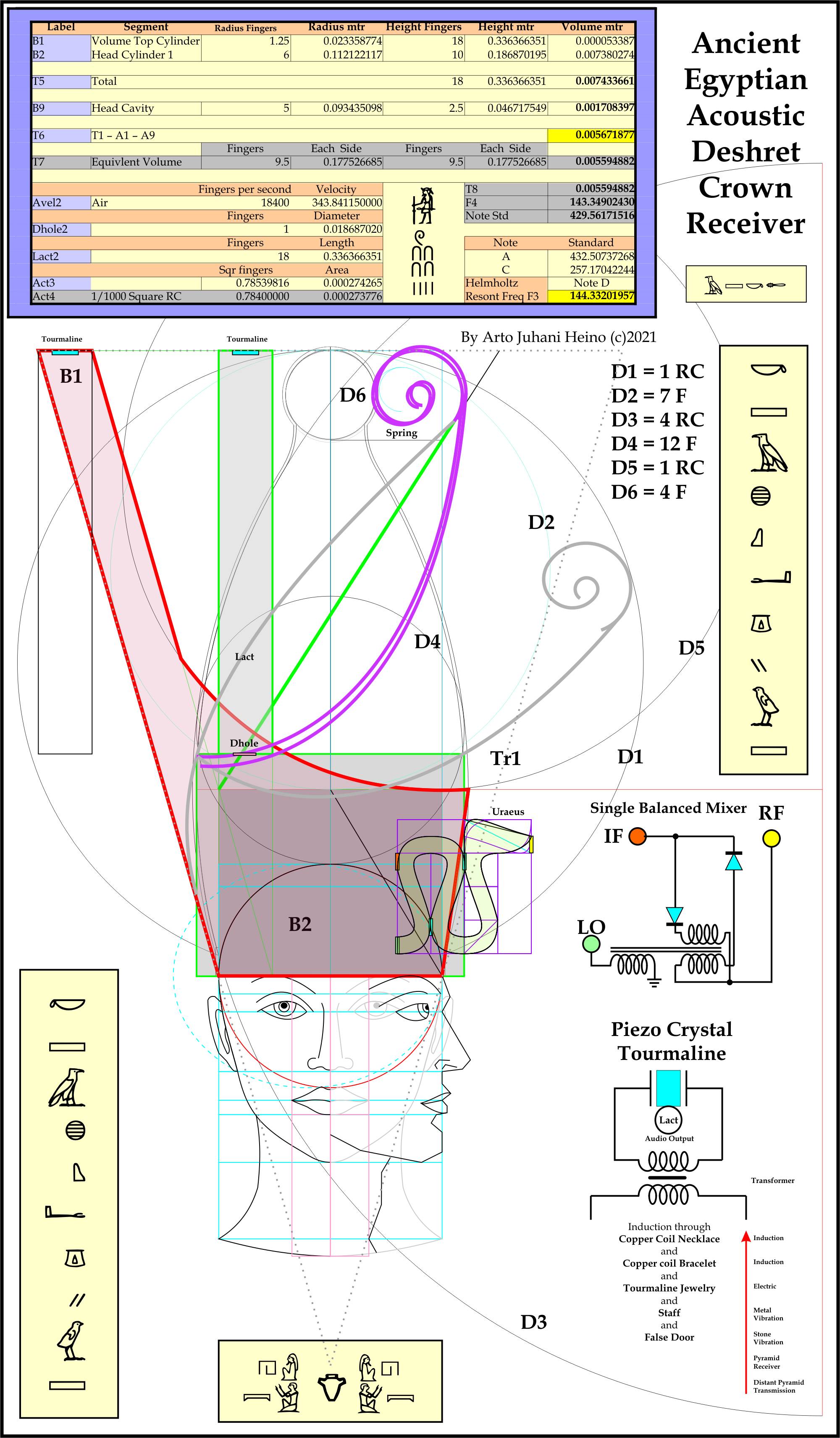
Here is the data for the Sonic Pyramid Field, the first graphic reveals the structure for the first section. The other table is the measure in Ancient Egyptian measure, note the Conversion to meters is 1 RC = 0.5232365464746810 Mtrs. These are my first data sets, excuse any errors, Regards Arto.
Looking at the White Crown of Upper Egypt (Hedjet, hdt) indicates a technological reasoning behind it design, yes I do not think they just randomly invented it without simple reasoning and logical inclusion. As with the other crowns they all served a similar function, one of communication through logical utility and natural means. “Per Neter”, “House of Nature”, the nature of sound, light and vibrations of communion to each other and other living beings. This is understood as the longitudinal vibrations of sound and of light, each only being a multiple octave distant from each other, one medium is the Ether the other is Matter (Air, Water, Earth).
The messenger of our time who understood this “Neter” was Nikola Tesla, in the past Christiaan Huygens was a proponent of it in his time and Roger Boscovich in his time as well. Fortunately you cannot fudge the longitudinal “neter” of sound, it is all around us and our ears and voices are organs we are closely connected to. On the other hand the fake Scientism movement which began in the early part of the 20th Century, which hijacked the symbols and contorted the mathematics to be some surreal multidimensional occult scheme. We are lucky that we have had some great minds and logical thinkers who knew the false paradigm was being perpetrated onto our scientific community.
As a Musician, I could recognise the acoustic volumetric of the crown almost immediately, that being in a vocal range. After taking great care to find the measure of what constituted the Resonator, I quickly found the design concepts that was used by the Khemtians. The next step was to look if there were schematics in any wall art, as possible translations of vibrations of sound to electricity and back to sound was taking place.
The fundamental wave length came from a careful measure using Google Earth was to reveal the base wave frequency that I should look at. After reading many volumes of Geological data regarding the Density, Bulk Modulus and Sonic Velocity of rocks of different genre, local to Egypt and other ancient sites, I can estimate the bedrock sonic velocity is usually around 5979.85 m/s, the Density about 3000 kg/vol and the Modulus is 10.7 Gpa, when translated to the Ancient measures, we have a Velocity of 80000 P per sec, a Density of about 2 Q/vol and the Modulus of about 1500. The distance from Senusret II Pyramid to The Great Pyramid is exactly 160000 Royal Cubits, simple calculations reveal that 14 seconds will transpire before your signal will be received and 28 seconds for the return signal, this could be considered a Time standard.
The Resonant frequency of the source to and from the destination = 0.0714285714 Hz
The Vocal Chord Range
= 65.714 – 4600 hz Wide Band = 131.43 – 2044.44 hz Medium Band = 262.857 – 920 hz Narrow Band
Male Speaking Vocal Range = 85 – 155 hz Female Speaking Vocal Range = 165 – 255 hz Children’s Speaking Vocal Range = 180 – 360 hz
The Crowns and head gear Range = 36 – 440 hz
The Wave Lengths WB = 343.841/65.714 = 5.232365 mtrs = 10 RC = 280 F = 343.841/4600 = 0.074748 mtrs = 1 P = 4 F
MB = 343.841/131.43 = 2.616194 mtrs = 5 RC = 140 F = 343.841/2044.44 = 0.168183 mtrs = 1 SH = 9 F
NB = 343.841/262.857 = 1.308091 mtrs = 5 LS = 70 F = 343.841/920 = 0.373740 mtrs = 1 D = 16 F
The design of the Hedjet Crown was a well drawn out study, I referred to many icons that show clear pictures, the first being the Narma Palette and many beautiful sculptures and large statues. It seems to have a slightly different size depending on the region and the Dynasty that had created the artwork. So instead of slavishly copying something that we had no sample of, with only diagrams or sculptured versions, I went with the most direct method, think like an Ancient and design like an artist of the time and build like an engineer of Khemet. As the Royal Cubit was the fundamental rule that all these ancient wonders that were created, I used my perfected measure of 1 RC (523.2365mm) as the foundation of design and engineering, also being 28 fingers (18.687mm), where I could use the finger as the smallest measure.
The large curvature of the circle D3 of the Hedjet is 4 RC, I could have chose 3 RC but the cavity would have been too small and the curve too tight, also if it was 5 RC the crown would have been to tall, 4 RC was the best fit that also matched the edge of D4, which is 12 F or 1 Small Span. The A1 dimension of 2 F was not a hard choice, it lined up to most crowns and was easy to pick, whereas the body had to be dissected to cylinders to get an approximate volume, using a basic form of calculus and the Egyptian measure I achieved a simple design tool that could be used on many semi-organic designs. The inside of the Hedjet could be two chambers or more, in line with the design of the cochlea, when unwound has two basic chambers, this could indicate a slightly modified version of my interpretation, which I will express in another design.
My intuition told me that I would arrive at a tonal resonance around the vocal region, being 95 Hz it was just about right for the low end of a set of large male vocal chords. The measure was the key, whole numbers of Fingers is the how we can design natural machines, like a resonator. The DNA understands these forms, your ears and your vocal chords are the result of this understanding, how can we imagine these were randomly adapted, they were designed by a master architect of the universe, we can only imitate its great design.
Here is is short list of Gems used by the Ancient Egyptians (PZ is the preferred piezo ):
Tourmaline Blue PZ Amethyst Purple PZ Sapphire PZ Emerald PZ Ruby PZ Diamond PZ Garnet Red Lapis Lazuli Blue Obsidian grey Carnelian Orange Jasper Orange Turquoise Blue Carnelian
All the crowns have the basic form of an acoustic device of some sort, this was their unique mastery of this most ancient technology and science, Tourmaline was the first choice for the Piezo crystal, this was one of the regular stones used in Egyptian jewellery and art.
Sound Refraction
The focal length of a spherical lens (measured from the surface of the lens to the focal point) is given by focal length sphere where r is the radius of the sphere, m1 is index of refraction of the surrounding medium and m2 is the index of refraction of the lens material.
r = Radius of Sphere m1 = Index of refraction of surrounding medium m2 = Index of refraction of the lens material v1 = Velocity of Sound of surrounding medium v2 = Velocity of sound of the lens material f = Focal length from the surface of sphere to the Focal point
f = r*(2-m2/m1)/2*(m2/m2-1) f = r*(2-v1/v2)/2*(v1/v2-1)
If the lens material has a greater velocity then it becomes a convergent lens and if it is less that it is a divergent lens.
Zp = Acoustic Impedance Piezo Electric Material Zl = Acoustic Impedance of Loading Material Wm = Matching Material Layer Wavelength
Best impedance match:
Wm/4 = Zm
Impedance of matching layer material is:
Zm = (Zp x Zl)^(1/2)
Wide band acoustic impedance:
Zm = (Zp x Zl^2)^(1/3)
Improving acoustic matching:
Zm1 = (Zp^4 x Zl^3)^(1/3) Zm2 = (Zp x Zl^6)*(1/7)
Mixing powdered piezo materials with hard resins and creating a polymer is one way of fabricating matching layers.
Hedjet Crown
This was the first I had seen that would work acoustically, using the Helmholtz resonator as the basic design to follow. The volumes are best approximated as the chambers are narrow band devices and not just singular tone, The narrow band fits the voice well, my criteria was to use it like a musical instrument, where pure tones resonate distinctly, a vibration from an external source being simple not highly modulated, one from the vibrations of a staff or device that has a limited tonal range. The connections to the circuit and ears are not included, these would be more decorative and need to be adjusted for the head of the user. The main chamber could be split in two, as per the uncoiled cochlea. I chose the size in accordance to the Royal Cubit as the standard, by it having direction relationship to the Longitudinal velocity of light. The original crown was worn by Narmer and he was a giant, so I figured this was the most suitable size, as I noticed the Hedjet sometimes seemed over size when the king was not as big in many wall carving. Later Hedjets could have been smaller, making the frequencies much higher than 95Hz.
Deshret Crown
This one was simple once I found the first crowns acoustic design logic. The spiral piece could be a hollow chamber as well, making it look like the cochlea, where adjustments to the tone and frequency could be made or even a direct contact to another acoustic vessel. The Green outlined section is the simplified version of the crown volumes that makes the mathematics much simpler. Tr1 is a golden triangle that was found after I had almost drawn the whole unit, it points to the heart, the size is 471/18 x 818/18 fingers = 488,977mm x 849.221mm. The Uraeus I put on the crown is mainly to show its location and design elements, the scale is not correct, it would be at least 1/2 to 3/4 of the size I have drawn.
Hathors Head Gear
This was a simple progression, now using the symbolic shapes of the sun disk and horns to create the necessary configurations. The C2 chamber in green is an approximation of the neck of the horn resonators. The P5, P6 and P7 are other positions the Piezo crystal could be placed and change how the horn chambers worked harmonically. The P6 is also connected to the main chamber, so a feedback will occur. The P7 connection is used when you use both horns, what you will get is one horn in compression while the other horn is in expansion, as opposite phases. P5 will drive the side horn but will also have a short wave of 1/7nth the of the wave length of the horn, thus giving you a complex sound wave. Tr2 is another golden triangle that I discovered after drawing most of the head gear, it points to the mouth, the size is 18.2 x 28 Fingers(1 RC).
Other Crowns and Head Gear
After intuitive generating these designs, I could see every crown and head gear designs were connected to the cochlea and other sound chambers. The feathered version of the Hedjet called the Atef Crown makes me consider that the internals as two chambers and the feathers as ticklers for a variety of harmonics. Amun crown has two distinct chambers, and it’s appearance is significantly like a straightened out cochlea. The Shuti Crown has spiral chambers(rams horns) which would be a shorter version than long straight chambers. The blue Khepresh Crown is much shorter and has a chamber as well, while the Cap crown has even a smaller chamber,
Each crown or head gear or combinations seems to indicate a narrow band of frequencies and could possibly be that each has a function of communication at those frequencies, where the deployment of signals were directed to those who wore a specific crowns or hats in a region. What I could gather by the wonderful hieroglyphs is that stock holdings were relayed among the Khemtian empire using false doors as exchanges with a schedule using specific times by officials with certain hats, which were regulated in a religious fashion to keep the communication channels linked up. The pyramids served to create, amplify and relay the complete network of acoustic signals around the empire.
The transmission of signals via a sonic device inside the sarcophagus like I have previously described would be linked to the regular acoustic carrier pyramid frequencies, with the use of a Sistrum as the calling ring when pressed against the walls in certain locations, like the false doors, when done at regular intervals to indicate a transmission signal.
The Uraeus is a 1 1/2 or 3/2 wave system, the locations of the Piezo crystal help with feedback tuning and aerial reception of Sonic frequencies, these would be coupled to the main acoustic chamber and also act like the diode mixer in radio when separating frequencies to be decoded. By the design it looks like a single balanced mixer, where the RF (Radio frequencies) is the Sonic wave and the LO (Low frequencies) is the voice and the IF (intermediate frequencies) are the carrier frequencies.
As this is still a working document, excuse any errors or omissions, but if you found this work of value please donate to keep this and other projects alive. regards Arto
An error has occurred; the feed is probably down. Try again later.
Join 130 other subscribers
Published material Link
Talking to the Birds
Book Available NOW
At Amazon
At Createspace
https://www.createspace.com/4513692
______________________
Cartoons
http://www.scribd.com/doc/106684504/Scraps-Sketches-and-Satire
_______________________
Magic Square
http://www.scribd.com/doc/33050524/The-Magic-Square-of-Three-Crystal