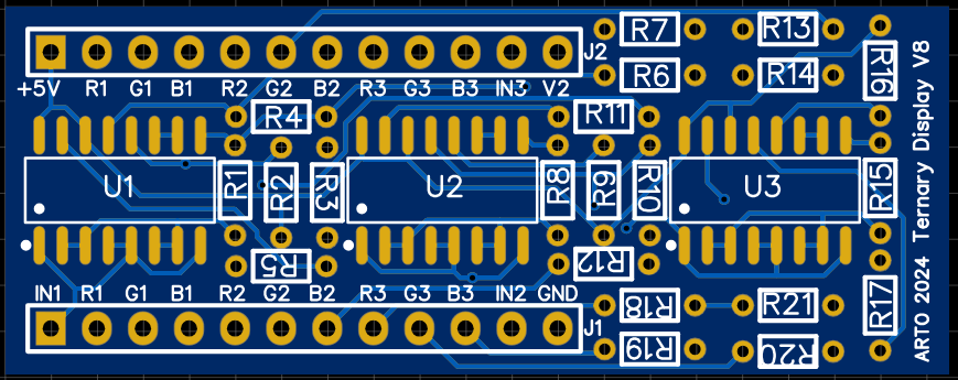
This board design concentrates on the 2 input Ternary Combinations.
I had made many Ternary Gates, here are 2 preferred designs using optical relays, using a 28 pin form.
The display units are less demanding and can be designed in many ways, here are 3 designs, using 24 pins.
The V9 Ternary display unit requires 100 ohm resistors before grounding, if you use V7 or V8 you can just use shorting wires if you requires them, or just leave in the 100 ohm resistors. ( untested)
First of all the 6 switched inputs relates to three 2 input gates which are arranged to give you a maximum of choice.
The first 2 inputs A1 + B1 are directly combined in C1 to create the 2 output gate, designed by the links you combine in 12 pin matrix on the right side of each TNG2-1 chip.
To make your life easier I have put a number of gates that you can use on the bottom of the main board.
The LED outputs are in three groups:
1] switched inputs (6) A1 B1 A2 B2 A3 B3 2] output from each ternary gate (3) C1 C2 C3 3] output from combinations of 3 ternary gates D1 D2 4] output from the last 2 gates E1
To understand the Ternary Gate link matrix, here is a legend:
The jumper settings allows 81 variations, in 3 blocks -1 to 27, 28 to 54, 55 to 81;
I set the basic set up as number 67 from the list above. There are only 36 link combinations that include all three outputs from gates C (they form a top/bottom symmetrical list). Here are the sets:
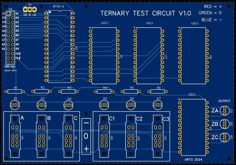
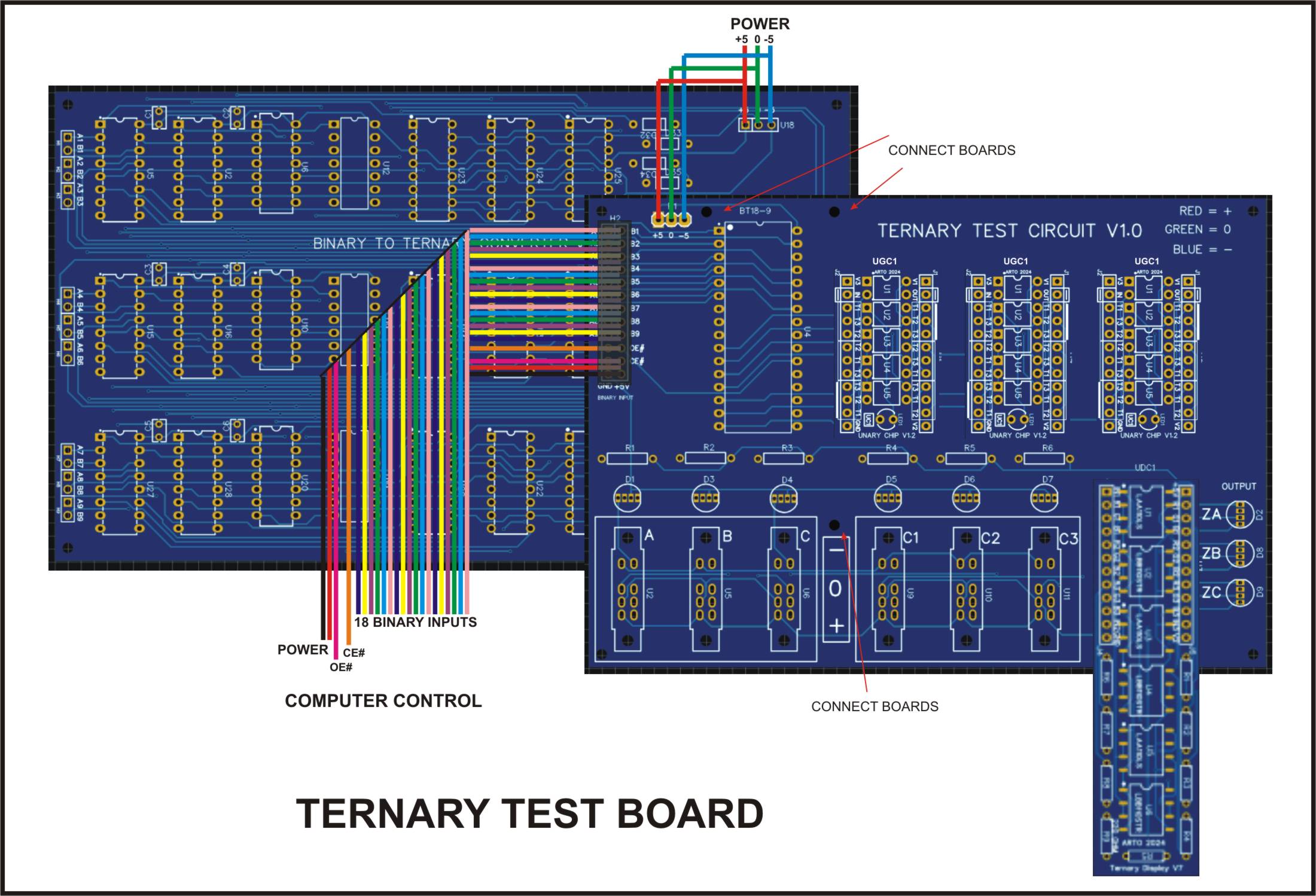
This board can accommodate 3 ternary chips the “BT18-9”, “UGC1” and “UDC1”, all of which are separate units, the BT18-9 needs either a set of ribbon cables with a socket or it can be directly connected with some HDR pins such as the connection diagram into the test board.
BT18-9
18 Binary paired Inputs (A1 B1) to (A9 B9) 9 Ternary outputs T0 to T8 OE# = output enable (you can set inputs then set to 0) CE# = chip enable (you must enable to 0 to start chip) +5V GND -5V
UGC1
1 Ternary input 1 Ternary output 1 led indictor of (-) 6 sets of programable inputs, in order
T1 T2 T3 T2 T3 T1 T3 T1 T2
T1 T3 T2 T2 T1 T3 T3 T3 T1
You can only connect 1 set at any one time, if you use a set of 3 jumper pins on all of the sets you could swap your combinations. These combinations will change your inputs into any one of six possibilities. This could also be done by using a analogue chip in a separate circuit.
UDC1
3 Ternary inputs 3 sets of 3 colour led outputs 3 sets of 3 colour led outputs (mirror of 1st set) So you could use these as Binary output switches or sensors as required. GND V1 = +5V V2 = spare 1 (-5v)
There are 3 ternary input switches (A B C) for all three RGB outputs (ZA ZB ZC) to function, there are also 3 selectors that need to be programmed first. Two of these are programmable by a binary source, while the other is by the onboard switches (C1 C2 C3). The current footprint of the display chip is 24pin pdip, even though the board is longer. As this is still only version 7, more work to do yet and I will eventually make it fit inside the boundary similar to the UGC1 board, on version 8 or 9. I am using optical relays in this design, something that I found useful in my ternary work.
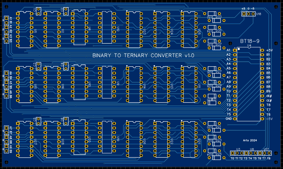
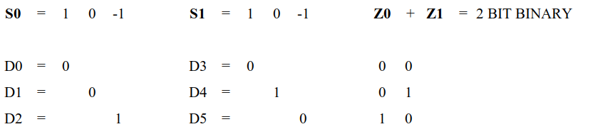
Starting from a Binary input where you have 2 bits to make a ternary trit:
00 = + 10 = 0 01 = –
The bit combination “11” is not valid and will not be used even though it is available as a binary output. The ternary converter ignores it.
Here are the 27 Unary gate combinations that are available and the binary combinations that will create them all. The UGI is the “Unary Gate Index”, numbering of all the gates in a system I have shown on my previous blogs.
Starting with the A1 and B1 as the first pair, then the A2,B2 then A3,B3, these three sets will give you a Unary set of 3 that will configure the basic Unary Chip “UGC1” to one of the 27 gates.
The second set A4,B4 + A5,B5 + A6,B6 will configure the next UGC1 gate. The third set are the switches C1,C2,C3 these will give you another UGC1 gate for you to use.
The outputs ZA,ZB,ZC correspond to the input data A,B,C, where your programmed UGC1 gate is being used to compute your result into the Z Led outputs. Where:
Red = + Green = 0 Blue = –
The input switches A,B,C,C1,C2,C3 also have RGB LEDs.
I hope this might start your interest in Ternary Logic and Computation, regards Arto.
** I have added UDC1 V8 to the Zipfile **
Ternary Test Boards PCB1D Zipfile
Al the PCB and Schematics for this project.
EasyEDA files only.
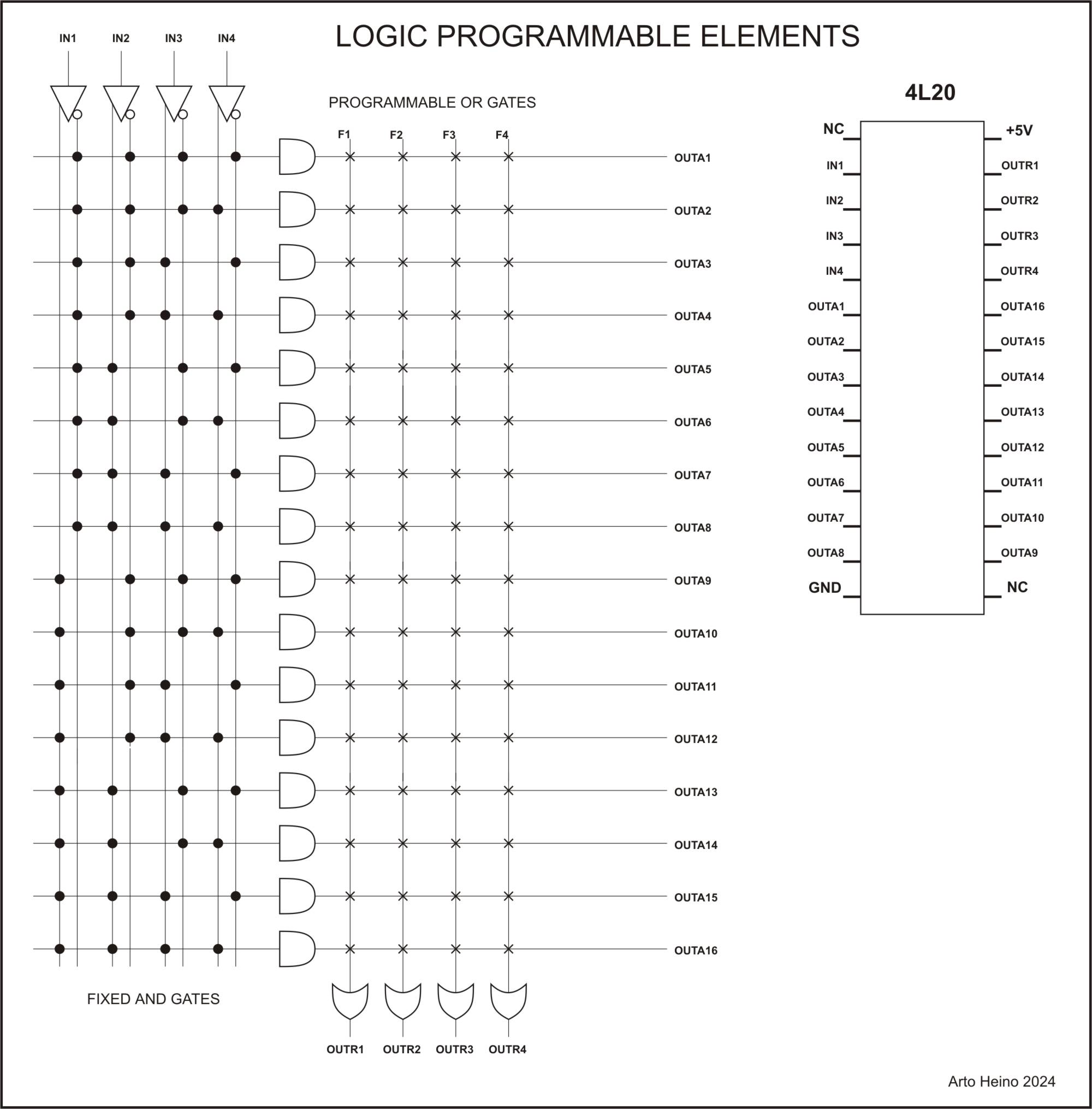
As a hobbyist I am always trying to work out how certain technologies function, so I decided to look into the PAL, PLA and any programmable logic arrays. So instead of using them as most technicians do I decided to create my own, by standard logic gates and switches, as I am just as interested in the why as the how.
These are my versions of Programmable Logic Arrays based on 74LS chips and 2 position toggle switches. I could try and replicate a standard PAL or PLE chip, but that would just clutter my simple approach as a learning tool. I made them so you can jumper the IC socket into to an existing circuit to test your programming.
LPA-4H10
Using AND/OR arrays, the AND array is either on(throughput) or off(made high) and the OR array is a fixed set to give you the maximum of multiple of outputs (6). My design is based on four 8 input AND gates, which are selectable by 8 switches, giving you a maximum of 32 switches. Using the 4 input bits and it’s inversion to give you 8 internal inputs for each AND gate.
IN1 x IN1# x IN2 x IN2# x IN3 x IN3# x IN4 x IN4# = OUTA1
Your input IN1 to IN4 are you only inputs, all the logic combinations are after your initial input.
AND Gates
2 INPUT, where A=INv and B=INw and Z=OUTAy (v = 1 to 4, w = 1 to 4, y = 1 to 4 )
AND NOT NOT AND AND AFBT ATBF NOR A B Z A# B Z A B# Z A# B# Z --------- --------- --------- --------- 0 0 0 1 0 0 0 1 0 1 1 1 0 1 0 1 1 1 0 0 0 1 0 0 1 0 0 0 0 0 1 1 1 0 1 0 1 1 1 0 1 0 1 0 0 0 0 0
3 INPUT
A B C Z A# B C Z A B# C Z A B C# Z ------------------ 0 0 0 0 0 0 1 0 0 1 0 0 0 1 1 0 1 1 1 1 1 0 0 0 1 0 1 0 1 1 1 1 1 1 0 0 1 1 1 1 1 1 1 1
A B# C# Z A# B# C Z A# B C# Z A# B# C# Z ------------------ 0 1 1 0 1 1 1 1 0 1 0 0 1 1 1 1 0 0 1 0 1 1 1 1 0 0 0 0 1 1 1 1 1 1 0 0 1 0 1 0 1 0 0 0
The abbreviations AFBT and ATBF was devised by me to simplify some of the less known logic gates that are available to the binary combinations. All these odd types of gates can be created with AND, OR, XOR, NOR, XNOR or NAND gates with an inverter on one of the gates as well. I don’t know how useful my ideas are to those Engineers who were educated in Digital Logic, but as an intuitive tool that I have developed, it has given me an insight into applying digital Systems to my Ternary work. As Ternary logic has a massive (19683) number of 2 input elements, your mind boggles at the idea of “Truelean Logic” as opposed to “Boolean Logic” which has only 16 two input elements. Here is the Matrix I developed when I sorted my relay logic elements, it clearly shows how it was developed.
AFBT (AfBt)
Z = (A = False = 0) + (B = True = 1) = True = 1 Z only equals True when (A = False = 0) and (B = true = 1) all the rest are False = 0. If you look at the A input as inverted you will have the same as standard logic, as such:
My Symbol: ____ A ----\ \ | \---------- Z B ----/____|
De Morgans Symbol2 Gated Logic _____ _____ A ----O| \ A ---|>O--| \ | |------- Z = | |--- Z B -----|_____/ B --------|_____/
ATBF (AtBf)
Z = (A = True = 1) + (B = False = 0) = True = 1 Z only equals True when (A = True = 1) and (B = False = 0) all the rest are False = 0. If you look at the B input as inverted you will have the same as standard logic, as such:
My Symbol: _____ A ----\ | | /---------- Z B ----/___/
De Morgans Symbol2 Gated Logic _____ _____ A -----| \ A --------| \ | |------- Z = | |------ Z B ----O|_____/ B ---|>O--|_____/
My Symbolism for multiple inputs
AfBCDEFGt

           *     *     *     *     *     *
Z = (A=0)+(B=1)+(C=1)+(D=1)+(E=1)+(F=1)+(G=1)=1

ACDEFGtBf

     *           *     *     *     *     *
Z = (A=1)+(B=0)+(C=1)+(D=1)+(E=1)+(F=1)+(G=1)=1

ABDFGtCEf

     *     *           *           *     *
Z = (A=1)+(B=1)+(C=0)+(D=1)+(E=0)+(F=1)+(G=1)=1
LPA Logic
The output from the AND array goes into a OR array that is set by 2 inputs using a OR combination, such as:
As you can see there are no more possible combinations than these six for a 2 input OR gate. Another added output is the ANDed output before the ORing which gives you another 4 outputs to use, giving you a total of 10 outputs.
Example 1a:
Here are the equations you can use, by using only IN1 and IN2 as your inputs:
So if you use two inputs, also using only 2 switchs F1 ans F2 of both inputs. Thus you get:
“#” = inversion
“^” = high = 1 (off)
OUTR1 = ((IN1 x F1) x (IN1# x F2^)) + ((IN2 x F1^) x (IN2# x F2))
When a switch “F” is on, then it equals the “IN” input. If “F” if off the it is high (=1).
If, IN1 = 1/0 and F1 is on and F2 is off (1), the rest of the switches are off (1) IN1(F3-F8). Every even switch uses the inverted version of the odd input going to the internal OR inputs.
also, IN2 = 1/0 and F1 is off (1) and F1 is on, the rest of the switches will be off (1) IN2(F3-F8)
IN1(F2) IN2(F1) = switch to high
             AND				OR
             _____
IN1 -0101---|  F1 \  	0101	             ______
            |      |------- OUTA1 ---0101 ---\      \
IN1 -0101--O|__F2_/ 	1111	              |      \
                                              |       \__OUTR1_1101
             _____		              |       /
IN2 -0110---|  F1 \  	1111	              |      /
            |      |------- OUTA2 ---1001 ---/______/
IN2 -0110--O|__F2_/ 	1001
This will give you output to the OUTR1 line, the OUTA1 and OUTA2. This is the output when you swutch IN1(F2) and IN2(F1) to high;
If IN1 = 0 and IN2 = 0 then OUTR1 = 1 , OUTA1 = 0 , OUTA2 = 1 If IN1 = 1 and IN2 = 0 then OUTR1 = 1 , OUTA1 = 1 , OUTA2 = 1 If IN1 = 0 and IN2 = 1 then OUTR1 = 0 , OUTA1 = 0 , OUTA2 = 0 If IN1 = 1 and IN2 = 1 then OUTR1 = 1 , OUTA1 = 1 , OUTA2 = 0
Where switch position “on” allows your input to go through the circuit, while “off” is only “high” (1) so the AND gate now is one less than your total maximum of 8. So if you switch all 8 to “off” this input will be only be a “1”, giving you a “1” on the input to one of the set OR matrix inputs.
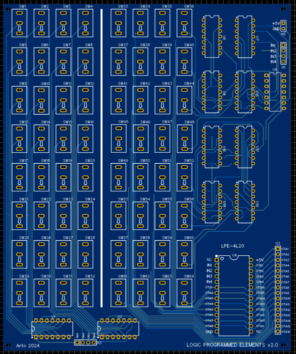
LPE-4L20
You get 4 inputs plus its internal inversions giving you 4 outputs (ORed) and 16 AND combinations. The off switch position is low, thus negating it throughput.
X = input o = inverted input
My first AND Matrix;
1 2 3 4 5 6 7 8 9 1 1 1 1 1 1 1
                  0 1 2 3 4 5 6
x x x x . x x . x . . x . . . .
. . . . o . . o . o o . o o o o

x x x . x x . . . x x . x . . .
. . . o . . o o o . . o . o o o

x x . x x . . x x . x . . x . .
. . o . . o o . . o . o o . o o

x . x x x . x x . x . . . . x .
. o . . . o . . o . o o o o . o
I was going to use this internal format, until I decided to use the standard PLE arrangement.
--------------------------------
   |   |   |   |   |   |   |
1 2 3 4 5 6 7 8 9 1 1 1 1 1 1 1		Net     AND Inverter output
                  0 1 2 3 4 5 6
. . . . . . . . x x x x x x x x   	H1  	A   1A
o o o o o o o o . . . . . . . .		U5_2	    1Y

. . . . x x x x . . . . x x x x 	H2	B   2A
o o o o . . . . o o o o . . . .		U5_4	    2Y

. . x x . . x x . . x x . . x x 	H3	C   3A
o o . . o o . . o o . . o o . .		U5_6	    3Y

. x . x . x . x . x . x . x . x		H4	D   4A
o . o . o . o . o . o . o . o .		U5_8	    4Y
So if you want to implement a 4 input XOR gate:
FnXOR = XOR (IN1 IN1# IN2 IN2# IN3 IN3# IN4 IN4#)
 =
(IN1 X IN2# X IN3# X IN4#) +
(IN1# X IN2 X IN3# X IN4#) +
(IN1# X IN2# X IN3 X IN4#) +
(IN1# X IN2# X IN3# X IN4) +
(IN1 X IN2 X IN3 X IN4#) +
(IN1 X IN2 X IN3# X IN4) +
(IN1 X IN2# X IN3 X IN4) +
(IN1# X IN2 X IN3 X IN4)
Switches used: (from 1 to 64) 5 9 17 29 33 45 53 57 – or – first column (1 to 16) 2 3 5 8 9 12 14 15 are ON all other switches are OFF
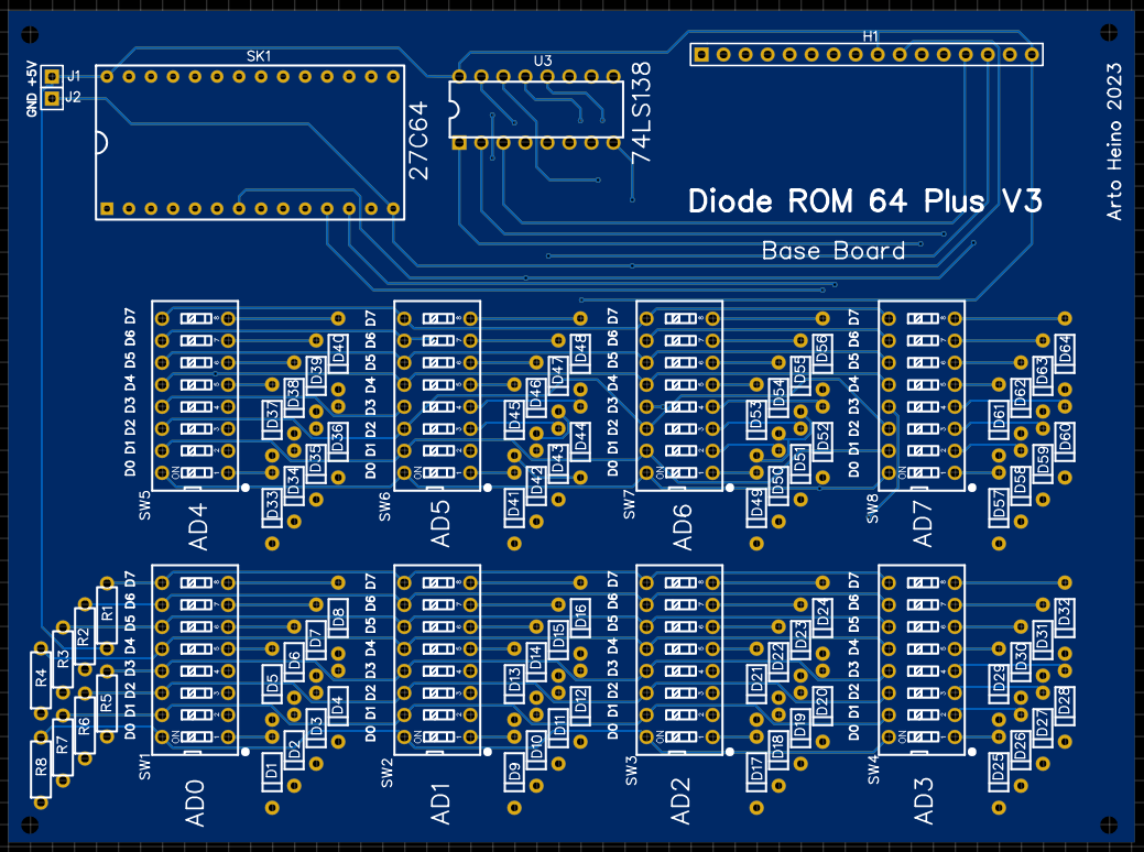
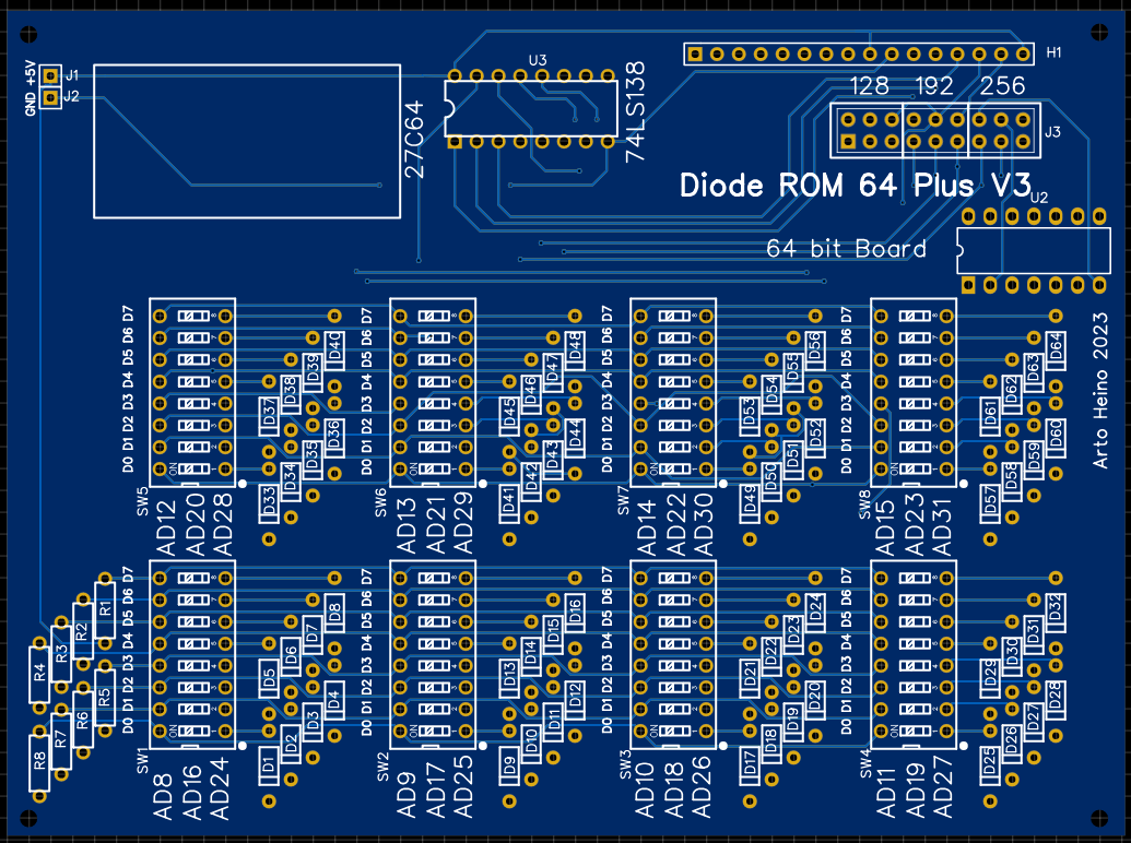
As my research moves along, I decided to create a Diode Memory unit first for binary use, before I implement the ternary memory version. I designed 2 types of boards, the first is the base board which is the first 64 bits or 8 bytes, the 2nd board can be stacked on top to create 128 bits or 16 bytes with more boards on top for 192/256 bits or 24/32 bytes. I will be building these soon, as these designs have not been tested yet, I suggest checking my work, I will confirm these in another blog.
The ROM choice was a 27C64 which is a 8Kx8 and is very popular, available in general stock and I will use it in further designs, the decoder is a 74LS138 which seems to be a great choice for this simple project. The only problem I had was the 138 has only 3 bits to decode, so I had to add a few extra bit of routing to create 32 bytes. The 138 has 3 enable lines GA_, GB_, G1, so the first block I put G1 high and GA_and GB_ would be enabled when both are low, these are from the A3 and A4 lines which are low. The second block I put GA_ low to ground with GB_ and G1 would be A4 as low and A3 as high. As you can see by the diagram I swapped A3 and A4 with GA grounded for the 3rd block, the last block I used an inverter on GB_ from A3 which must be high,
If you are not using 32 bytes then you can ignore the 74LS04 connection. To use each block you must bridge the labelled connectors with jumpers. The Parts list for 2 boards are:
SK1 = 28 pin DIP socket with extended legs
H1 = 16 Pin socket with extended legs x 2
U3 = 74LS138 x 2
R1-R8 = 10K resistors x 2
D1-D64 = 1N4148 Diodes x 2
SW1-SW8 = 8 sw DIP x 2
J1-J2 = Pin for Power x 2
Each corner has 2mm holes , add crews and extended legs as needed x 2
If you choose to build it, you will be limited to 32 bytes. To test the unit you could plug it into to a EPROM reader. My next version should allow up to 256 bytes or more. Regards Arto.
Diode ROM PCB1C Zipfile
All the PCB and Schematics for this project. EasyEDA files only.
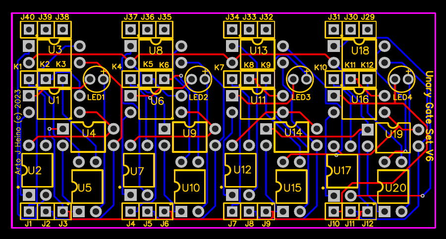
To start the journey of discovery, we must have all the building blocks and tools ready to use as creativity requires a selective group of useful mechanisms to achieve a modicum of feed back to keep the momentum going forward towards interesting and useful discoveries. The Ternary building block are here, along with a Binary controller that you can use to design your Logic elements as needed. I have shown previous Unary gates and they are still usable in these designs. I decided to put 4 gates in one unit so wiring can be simplified when you create the 2/3/4 input gates. For a 2 input gate you need 3 gates for the columns and a summing gate and 3 gates for the rows a summing gate for the rows and the result. This makes it simpler, you will only need 2 unary boards for an 2 input gate, a base board was designed to make this easier, these can be stacked, as high as required.
Parts List for each Unary Gate V6
U1,U3,U4 _________G3VM-353A U2,U5 ____________G3VM-61A1 U6,U8,U9 _________G3VM-353A U7,U10 ___________G3VM-61A1 U11,U13,U14 ______G3VM-353A U8,U15 ___________G3VM-61A1 U16,U18,U19 ______G3VM-353A U17,U20 __________G3VM-61A1 LED1,2,3,4 ________3mm Blue 36 x ______________Male/Female headers 20 x ______________4 Pin sockets (if required) 1 x _______________Unary Board V6
Parts List for Base Boards
4 x _______________24Pin Fmale Header 8 x _______________3 Pin
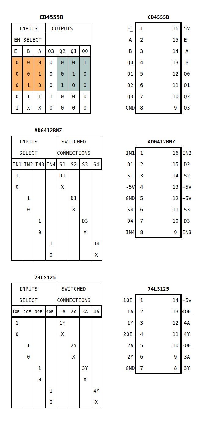
Parts List for Binary to Ternary Gate Selector Board
6 x _______________CD4555BE 9 x _______________ADG412BNZ C1,C2,C3,C4,C5,C6 _100 nF Caps D1-D12 ___________1N4007 D19,D20,D21,D22 __1N4007 1 x _______________LM7805 1 x _______________LM7905 C7,C10,C12,C22 ___47uF Electrolytic Caps Led1 _____________Led R1 _______________1K 3 x _______________6 Pin 3 x _______________5 Pin 15 x ______________8 Pin Dip 1 x _______________7 Pin Dip 1 x _______________74LS125
1 x _______________LAA110LS 1 x _______________LBB110STR 3 x _______________220 Ohm 3 x _______________1xPin hdrs 2.54 1 x _______________4 pin hdr 1.27 1 x _______________RGB PCB board
Parts List for TMS9995 Board
1 x ________U8 ____74LS138 1 x ________U5 ____74LS32 1 x ________U6 ____MAX232CPE 1 x ________U7 ____TMS9902 1 x _____U11+U12__TMS9901 x2 1 x ________U1 ____TMS9995 1 x ________U4 ____74LS04 1 x ________U3 ____62256-07 SRAM 1 x ________U2 ____M27C256 EPROM + Binary Data Cortex + Terminal 1 x _______________DB9 RS232 RA port 1 x _______________Header 6 Pin C1-C8 ____________100nF C11,C12___________100nF C16 -C20 __________1uF Electrolyticn R1________________10K R2 – R6____________1K C13, C14 __________15pF X1 _______________12 Mhz XTAL 1 x _______________LED21 LED indicator 1 x _______________SW4 Micro switch C15 ______________10nF 4 x _______________10 pin RA Male Pin Headers 1 x ________U9 ____LM7805 C22, C23 __________47Uf DC1 ______________9v input Jack 3 x________________40 Pin Dip 2 x _______________ 28 Pin Dip 2 x _______________ 14 Pin Dip 2 x _______________ 16 Pin Dip 1 x _______________ 18 Pin Dip 1 x _______________TMS9995 SBC PCB Board (Conner Stuarts Design)
Boards
Unary Gate Base Board V6 Unary Gate Base Board Singles V6 Binary to Ternary Gate Controller V1 Ternary Input Switches Ternary Bit Display TMS9995 SBC
Each Unary board consists of 4 separate Unary Gates they can be used as a set or individually, depending which base board you use.
The Unary Gate Base Board has been configured as a 2 input gate A, B and the result in C.
The Unary Gate Base Board Singles is configured to use as either a 2 input gate by wiring it as required or as single chains or groups.
J1, J4, J7, J10 are your ternary inputs, while J2, J5, J8, J11 are your outputs to each gate.
K1, K2, K3 are configurable with J40, J39, J38 as a matrix to give you all 27 Unary configurations. The interconnections are configurable with a small 6 pin cross connected board, or you can use jumper cables if you choose.
Controller Board
This has a 12vac input and 18+3 pin binary input and a 3 pin ternary output. It was designed to connect to a TMS9995 SBC with CRU outputs and have software to control the gate configuration in hardware.
With Five Boards there are 45 binary controls which will give you a Ternary Multiplexer made of five 2 input gates and 3 Unary gates. Once you have tested and configured your logic, then you can use the base board with plugin matrix connectors as your final gate design.
Setting Your Bits
H1, H2 and H3 are your binary control bits to select each gate type. You select 6 bits to as either decimal or Hex to each unary port. I added U28(74LS125) and U29 3 pin header which is used to switch each gate on, under software control as required.
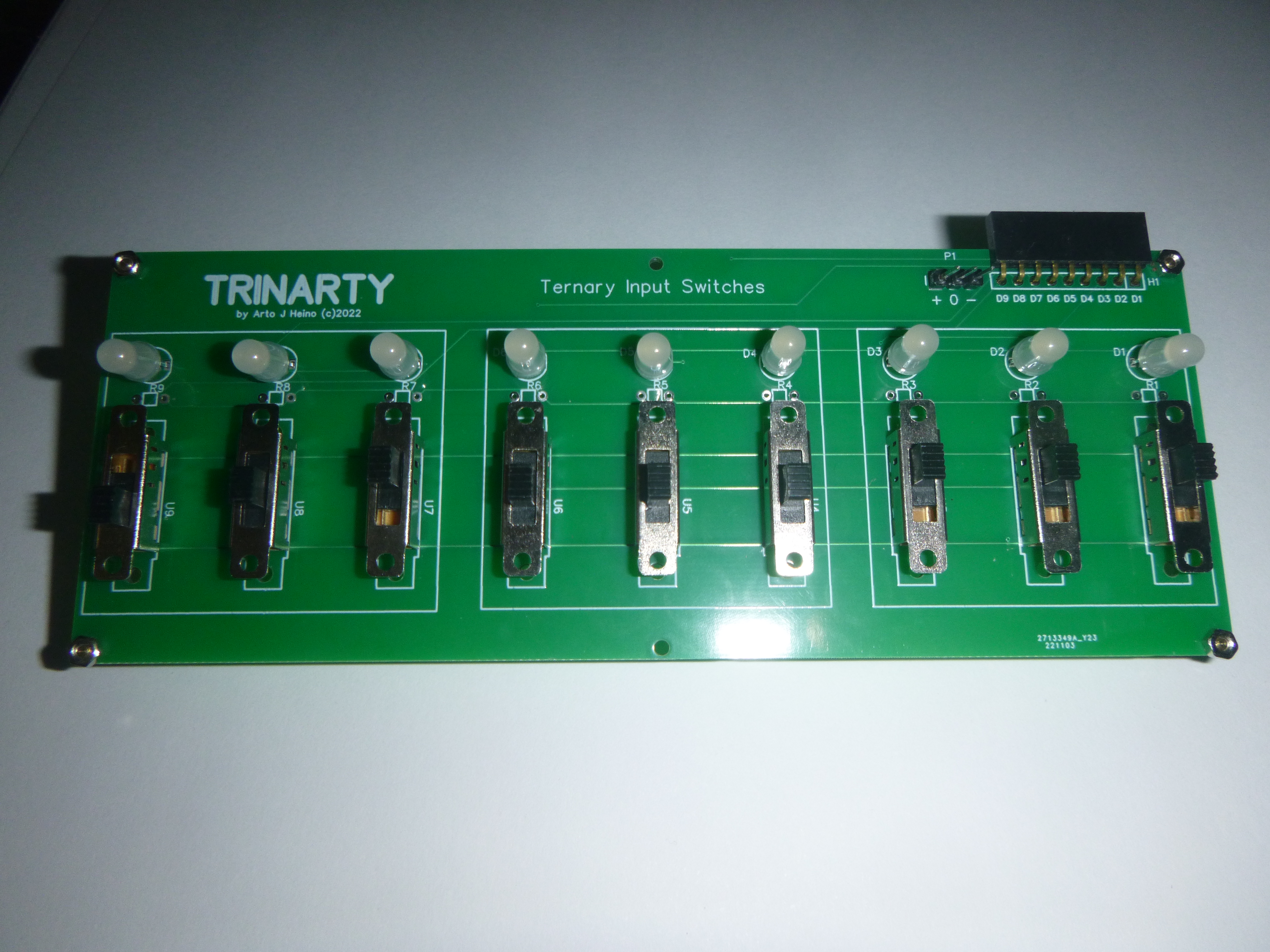
Ternary Input Switches
This board has 9 ternary outputs and can be used to control the A+B inputs on the Unary boards. There is 9 RGB indicators for the slide switches, Red = +5v , Green = 0v , Blue = -5v.
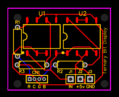
Ternary Bit Display
This small board gives you a visual indication of your output bits, Red = +5v , Green = 0v , Blue = -5v
Listed below is the Program to control the Ternary Gate Selector. If you want to attach more Selector boards you will need to expand the CRU outputs. I have left the header J5 to allow CE for more TMS9901 to be added at some point. The next version will also have have mounting board for 4 more chips, giving a total of 96 outputs.
Where 21 are needed for each 2 input gate, this allows control of 4 2 input gates, 84 pins , leaving you 12 spare pins for other controls.
This is a Cortex Basic program to control one two input gate.
8 REM TERNARY GATE CONTROL 9 REM *** BY ARTO HEINO 2023 ** 10 REM OUTPUT ON 9901 PORT BIT 0 to bit 20 (21 BITS) 11 REM TO CONTROL TERNARY 18 BIT GATES + 3 BIT CONTROL 12 REM 13 REM SETUP BASE ADDRESS OF 9901 to 64 decimal = >0040 HEX 14 BASE 64 15 DIM TR(27,6) 17 REM DISABLE EACH CD4555BE CHIP 18 CRB(16+18)=0 19 CRB(16+19)=0 20 CRB(16+20)=0 24 REM LOAD 27 TERNARY GATE BIT DATA 25 RESTORE 27 FOR Z=1 TO 27 28 FOR X = 1 TO 6 29 READ TR(Z,X) 30 NEXT X 31 NEXT Z 32 REM SELECT 3 GATES 33 FOR A=1 TO 3 36 PRINT “COLUMN “; A 38 PRINT “SELECT GATE 1 TO 27” 39 INPUT GT 40 IF GT<1 OR GT>27 THEN GOTO 38 42 FOR BT=1 T0 6 45 REM SET HIGH OR LOW 48 CRB(15+BT+(A*6-6)) =TR(GT,BT) 56 NEXT BT 57 NEXT A 60 REM ENABLE EACH CD4555BE CHIP 61 CRB(16+18)=1 62 CRB(16+19)=1 63 CRB(16+20)=1 64 END 65 REM DATA FOR GATES 66 REM H1 + H2 + H3 101 DATA 0,0,0,0,0,0 102 DATA 1,0,0,0,0,0 103 DATA 0,1,0,0,0,0 104 DATA 0,0,1,0,0,0 105 DATA 1,0,1,0,0,0 106 DATA 0,1,1,0,0,0 107 DATA 0,0,0,1,0,0 108 DATA 1,0,0,1,0,0 109 DATA 0,1,0,1,0,0 110 DATA 0,0,0,0,1,0 111 DATA 1,0,0,0,1,0 112 DATA 0,1,0,0,1,0 113 DATA 0,0,1,0,1,0 114 DATA 1,0,1,0,1,0 115 DATA 0,1,1,0,1,0 116 DATA 0,0,0,1,1,0 117 DATA 1,0,0,1,1,0 118 DATA 0,1,0,1,1,0 119 DATA 0,0,0,0,0,1 120 DATA 1,0,0,0,0,1 121 DATA 0,1,0,0,0,1 122 DATA 0,0,1,0,0,1 123 DATA 1,0,1,0,0,1 124 DATA 0,1,1,0,0,1 125 DATA 0,0,0,1,0,1 126 DATA 1,0,0,1,0,1 127 DATA 0,1,0,1,0,1
Here is the layout for the SBC and the Ternary Gates.
An alternative design without the SBC and just putting units together.
Here are a few pictures regarding some of the components.
This is the CODE for the 27 selections of Unary gates, H1,H2,H3 CRU outputs.
Here are the PCB’s for the Basic boards.
If you want to see more of this type of content, I would appreciate your support to help pay for more original designs and parts. I hope you enjoy this work, regards Arto.
Ternary PCB1A Zipfile
All the PCB and Schematics for this project. EasyEDA files only.
To be clear the multitude of Ternary 2 input gates is a gift to the creative mind, I have written a program that enumerates all 19683 and deemed all of them useful. An example of this is gate 2272 (TAB-index), which is “Tautology” or all “+1”, so any inputs at A and B results in +1 on the output. You might say what is the point of that? Only now it acts like a buffer or a line driver, so it serves a “function” in a ternary circuit or a re-encoder in a more complex circuit. After deciding what is needed to develop a Ternary computer, I first looked to the 27 Unary gates and the all gates that are commonly used in binary circuits, like AND, OR, NAND, NOR etc…which there are a total of 16 and which 6 are deemed the most useful.
Here is the complete set of Binary Relay Logic
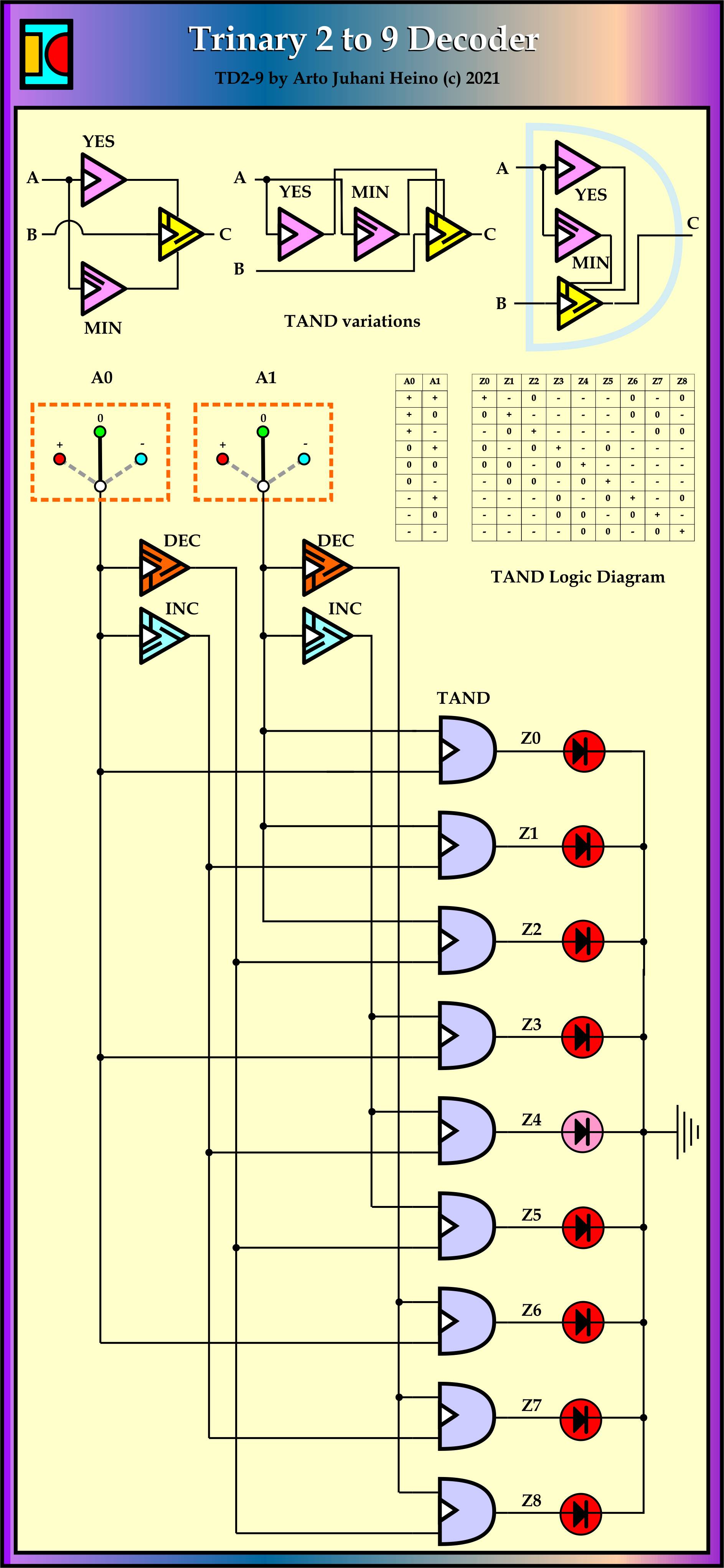
Exploring the Trinary logic opens a whole new way of seeing and thinking about computer architecture. For example a multiplexer is a most versatile device when designing circuits so I chose to explore this device to see what can be learnt from applying ternary logic to its internals. In a previous post (https://artoheino.com/2021/05/04/the-2-to-9-decoder/..) I showed my crafted and workable TD2-9 (2 input to 9 output) decoder. this will be the starting point of some new discoveries.
First lets go back to the simplest version the TD1-3 decoder:
I chose this one mainly due to the fact it can be used to decode Ternary to Binary, so one input from a Trinary based system can produce 3 signals to control a Binary based chip. So a mixture of Binary and Trinary is not difficult to attain.
Here is an example of one of my Binary to Ternary Interfaces based on a Analog Devices chip.
I have used a spread sheet to design the small Unary modules and 2 input Ternary Gate modules to develop these designs, they were based on the Ternary Relay designs I have outlined in my previous work.
The spread sheet model has helped me in developing combinatoric circuits and ensure consistent logical flow, as this is a new technological playground and has some crude pointers and intellectual fences to overcome. As the diagram of the 2 circuits show, we can decode with positive or negative numbers without the binary load that is usually a constrictive affair and become overly complex.
After much mind bending Ternary Logic visual calculations and pattern recognition, here is the First Ternary Multiplexer, TM3-1 with a future TM9-2, TM27-3 and TM81-4 as simple extensions. Where as the Binary can only achieve 2-1, 4-2, 8-3 and 16-4, so imagine how versatile these gates can be.
With this TM3-1 you could create a Ternary to binary converter, by using two of these
A Binary to Ternary converter is also possible:
They can also be usable as a 2-2 Encoder in binary:
Also by cascading the TM3-1 you can create the TM9-2.
Choice of Unary Operators
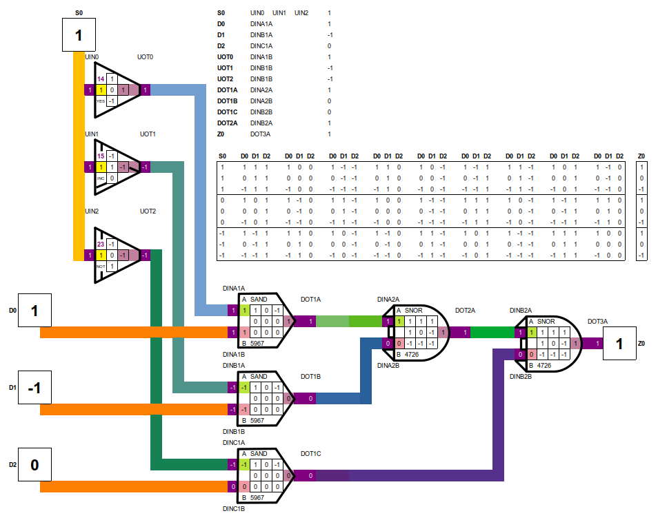
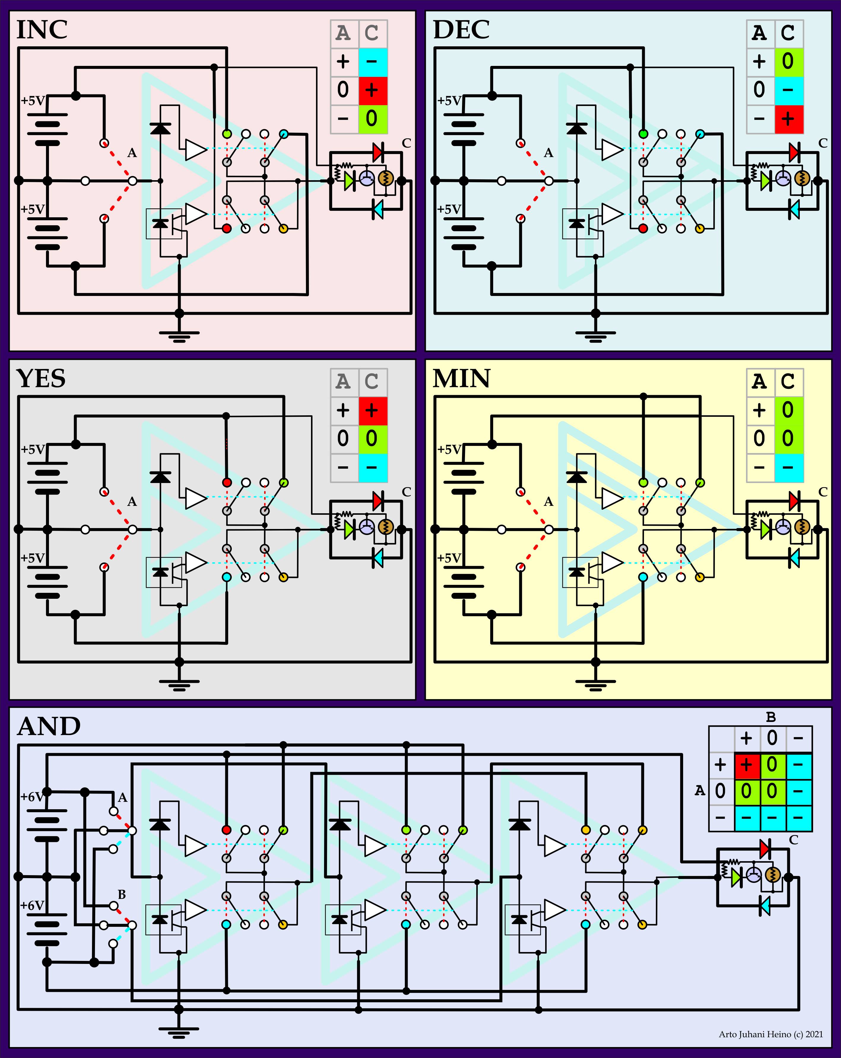
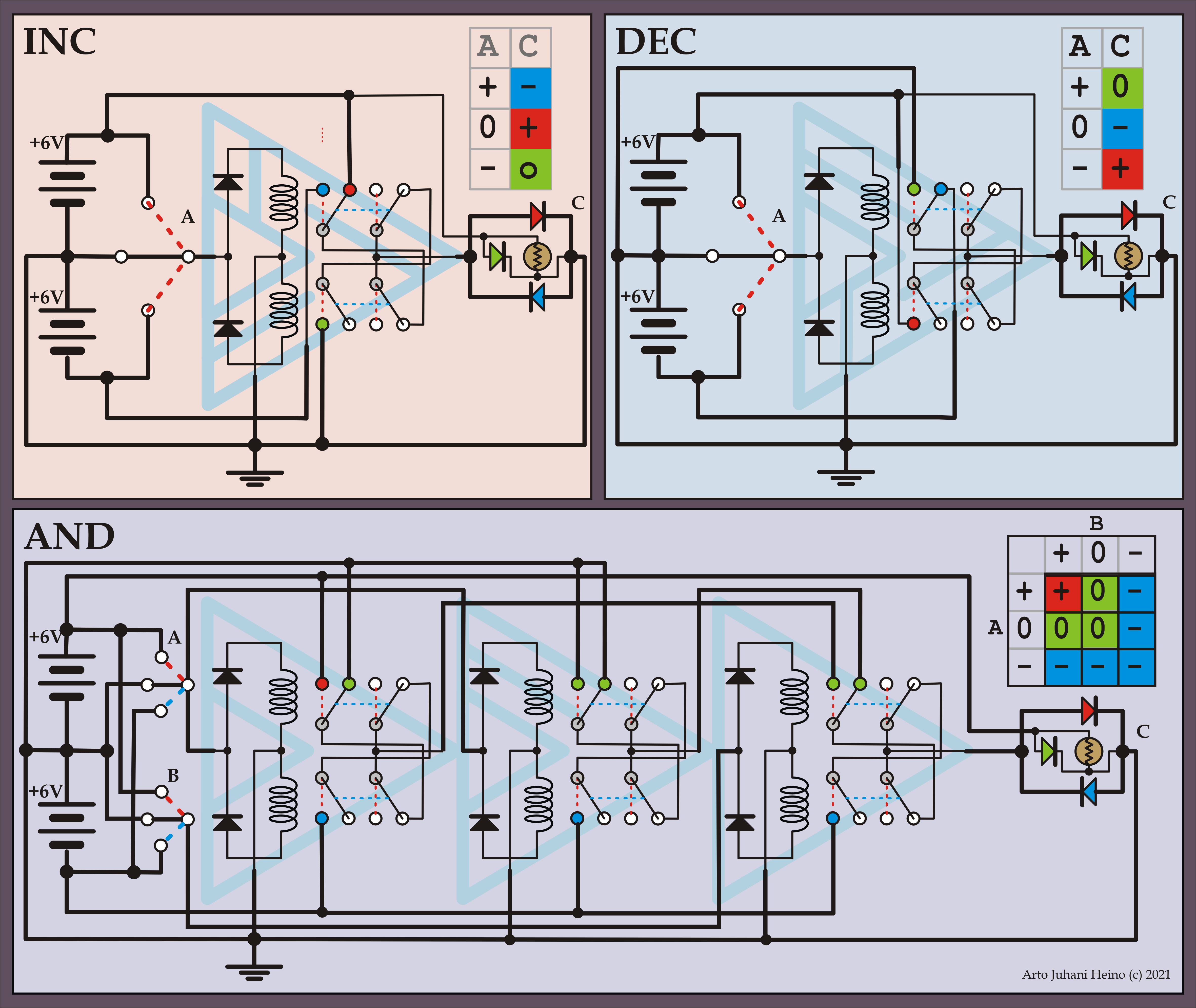
Using the binary combination of AND plus OR gates, I first applied the binary equivalents of the Ternary gates to create the Multiplexer but found the Ternary logic would not cooperate as easily as binary. This is when I realised that the ternary system would have a simpler gate choice to achieve the same result. Instead of TAND I used SAND, which has a simpler matrix, while the DNOR is similar to the TNOR gate. This gave me the start, which later I found that VAND and LAND gates also work.
Ternary 2 input Gates
Ternary Converter
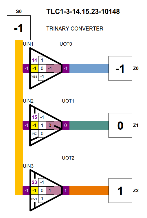
During these discoveries, I realised a ternary converter would be useful by itself. The numbering system describes the 3 gates and the 2 input equivalent.
Example:
TLC1-3-14.14.23-10148 TLC = Ternary Logic Converter 1-3 = 1 input 3 output 13.15.23 = Unary gates used 13, 15 and 23 10148 = The 2 input gate number equivalent 1 to 19686
Hardware Versions
After many attempts to make these circuits simple and easy to follow, I decided to concentrate on the relay versions but started using Photo-MOS Relays instead. This I found to be advantageous as the noise was eliminated and the current consumption decreased with the bonus of high speed. I would like to see a Photo-mos version of Programmable Logic, this would create a whole new industry, as the Photo-mos relays are already a mature technology today.
There are many manufacturers of Photo relays, lets look at the IXYS lettering, this will simplify your creative pallet. NO = Normally Open, NC = Normally Closed.
IXYS
LAA 2 in NO + NO 2 out 8 pin Dip
LBA 2 in NO + NC 2 out 8 Pin Dip
LBB 2 in NC + NC 2 out 8 Pin Dip
LCA 1 in NO 1 out 6 Pin Dip
LCB 1 in NC 1 out 6 Pin Dip
LCC 1 in NC + NO 2 out 8 Pin Dip
I opted to use the DIP 4 as well, as this would give me a more flexible layout and get different brand parts sourced and tested.
These designs cover the scope of mechanical relays, where you can configure SPST, SPDT, DTSP, DTDP different combinations, you can also have the current flow in either direction or as in neutral where there is no action to trigger the relayed combination.
in long hand: If A1 x 10 + A3 =11 then E2 Display Value = B1
Where you would normally write
If A1 = 1 and A3 = 1 then E2 Display Value = B1 By multiplying A1 by 10 then I can add the two the values without an a “AND” logical statement while keep track if it is true or not.
Example of A3 = 1 Say if A1 = 1 then A1 x 10 + A3 = 11 A1 = 0 = 1 A1 = -1 = -9
Also if A3 = 0 Say if A1 = 1 then A1 x 10 + A3 = 10 A1 = 0 = 0 A1 = -1 = -10
And finally if A3 = -1 Say if A1 = 1 then A1 x 10 + A3 = 9 A1 = 0 = -1 A1 = -1 = -11
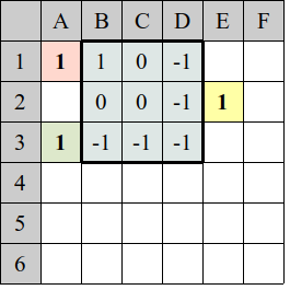
So you can see that the “+” in the code means “OR” , so now you have a truth table with 9 unique values. -11 -10 -9 -1 0 1 9 10 11 .The pointers are the input at A1 and A3 which define the value at E3 , altogether these are the general Logic Inputs of A B result in C.
The code for the Unary input was much simpler.
= IF(A2=1,B1) + IF(A2=0,B2) + IF(A2=-1,B3)
As you can see it is vital that your two input gates are in the correct order where as the binary version does not have that problem. Your A and B inputs and the coding of your ternary signals have a specific order which is determined by the original Truth table orientation. The convention I call “Natural” (T1) is “+ 0 -” and the Truth table is “A” rows top to bottom and “B” columns is left to right. The other options, which I have found among other ternary researchers are listed here:
By this table you can see how this effects the look of the Truth Table. So as in human relations we also have different languages in communicating, translating will not be difficult as these ideas are universal. The Non-Balanced (0 1 2) might not be as easy, as these now become arbitrary according to the designer, they might consider the “switched P” (0 + -) used as “0 1 2”, where as the “Natural” being “+ 0 -” and the equivalent would be “1 0 2”, a very confusing translation would make it difficult. This ordering is related to the voltage levels from 0 volts to 1 volt to 2 volts, this would be articulated in hardware making it incomparable with the Natural order and only interfaced through a translator. The Natural system also easily accommodates the AC wave and can be used as a clock without much difficulty.
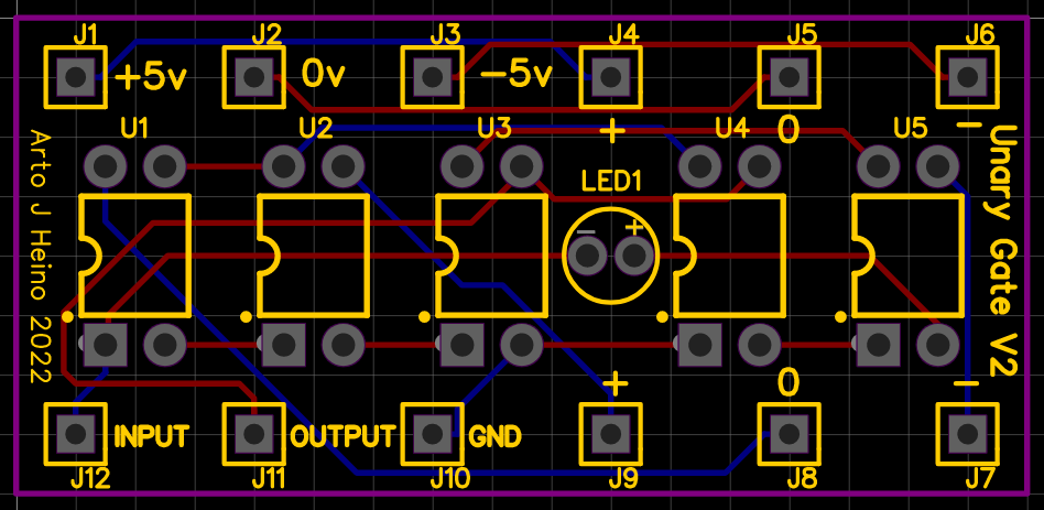
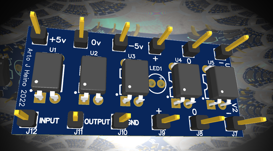
A Unary Gate Chip
The idea was to make a 12 pin bread board ready plug component that could be used to create gate combinations and test the results. Here is the UGC-V2 and a plug in header to change the Unary gate number as required. The plug-in header sits on top of the the J4 to J9 pins, it allows you to use all 27 gates. The unit is 20mm x 43mm and the plug is 20mm x 20mm.
Unary Gate Chip
I hope this spurs some interesting Ternary work and we might see a bright future in using “LIGHT” as the interface between the old Binary Paradigm to the new Trinary way of doing things. Regards Arto.
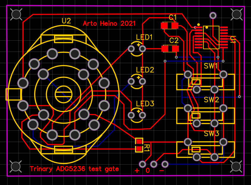
Rather than try to instigate the trinary action directly from the positive, neutral and negative charges, I have simplified it by setting the switches using only the positive rail and neutral before I have set the Unary Gates, using a ADG5236 Analog switch chip. This is only a testing measure to get all the gates ready for integration into combinatory sets like Tand and Tnor. You can say combinatory only in Ternary because each two input gate is made up of three Unary gates from a pool of 27, while each Unary gates is made up of three switched sets, sometimes as two pairs of DPDT while one is redundant, due to the lack of physical trinary switches available on the market.
I have tried not to compromise on either side of the switched in/out design, still we need to move these ideas forward so we can find interesting and valuable Ternary circuits that can accomplish much and more of what its little Binary brother has done in the last 80 years. The use of CMOS, PMOS, NMOS have been used successfully by many inventors to create Trinary circuits but have never been popularised due to the logical tangle of the unknown element “0”. This by philosophical terms is the “unknown”, “undefined” or “undecided” element, as binary has either Yes or No to which there is an easy determinate path to follow, no questions about a vague unknown.
This dilemma of the neutral place where indecision is its home, is merely an illusion that has been created by a physiological inability of our mind to see it any other way. I offer a simpler approach where S. C. Kleene, Post, Lukasiewicz and others has written much on the mathematics and semantics of this, where as I see it as a natural condition of our physical universe. The Earth is the simple model I follow, where the positive charges are above us and the negative charges are below us, while we stand on the neutral ground. This simple model also works for water and any other boundary situation where “0” is now the path of all connections made by its very nature, a skin if you like. (as above a mirror as it is below). Indecision is not unknown, it can be weighed just as gravity can be defined by units being weighed, a heavy object as opposed to a light one.
Much has been written about mathematics of ternary and it has its advantages over binary for sure, here is some simple arithmetic. Again I follow my simple model:
There is a simple and enduring beauty using trinary logistics, you never end up in a lock up situation, due to the neutral line where it can always carry its logic to a complete solution. The binary has the problem of only having a “true” and “false” narrative, where that is not how nature works at all.
The early Atomic physicists had to resort to phantoms of matter such as “Electrons”, “Neutrons” and “Protons”, these are mere conventions of usage not a reality of our universe. They used these mnemonic devices to solve abstractions they did not fully comprehend. Charge is all we really know, sadly the Ether was incorrectly dismissed in the 20th Century as the carrier of all the physical universe, not so, as we should simply state that charge is one of the different conditions of the Ether. This also makes the Ether as a neutral state, thus making it the default condition of everything that is not moving, or charged in any way, while Gravity is the Pressure of the Ether on all Mass.
Once Trinary thought is used in all circumstances, War, Famine, Invention and Mans ailing conditions will improve beyond mere Utopian dreams. False narratives and political agendas will be nothing but illusions we will all see through and will serve no purpose in our pursuit of our quality of life and living. The Us and Them syndrome are but Marxist drivel used to divide our sensibilities against the true knowledge of our existence.
Trinary thinking no longer separates us into “Right” and “Wrong”, “True” and False”, “Yes” and “No” but introduces gradations of wisdom and experience. I ask is it wrong that a bird can walk while it is only known to fly in the minds of many. Is the colour of the sky Blue when we see it as Red, Orange and Yellow at other times. Binary thinking divides our perceptions along a boundary, this boundary is the “Undecided” or Neutral line which we will now understand in Trinary thought, as the connector of everything. In electrical engineering it has always been called “Earth”, “Common” or “Neutral”.
Art precedes science just as culture precedes politics, this is why “reductio ad absurdum” of modern philosophy is a regressive step with the binary decision trees built from notions of “Left” and “Right” factions are nonsense and are a danger to our own survival. The Quantum arguments currently exploited by “Modern Science” are but Binary semantics made into a religion, called “Scientism”. The rulers of our lives only require serfs not thinking individuals, who have, graduations of thought and experience where true diversity only exists when we are allowed to think freely.
Addition of Trinary
+ add + = +-
which is
1 + 1 = 2
+- add +- = ++
which is
2 + 2 = 4
so if “-” = -1
then
– add – = -+
which is
-1 + -1 = -2
Try
-1 + 1 = 0 or 1 – 1 = 0
which is
– add + = 0
So a balanced ternary system is similar to the way we use electrical charge as well.
Here are the diagrams from my work, it will be included in my next volume “Talking To The Birds, Volume II”, coming soon, regards Arto.
The last two post were my personal dialog with Trinary procedures so I can start to create complex decision trees that can act in a intelligent and logical way. These are the beginnings into a natural engineered form of intelligence, I dare not say AI as these ideas are not artificial, they are natural only non living.
I went back to some of my work with the DG series of chips so I could make an interface board for the Led Matrix. I could design it with relays but decided that it would be great to see other options for Trinary design. Once mastered, an ALU would be the first step, maybe with many extra functions that binary ALU’s struggle to implement. I hope to add a Trinary version of Quantum Arithmetic built from these gates. (Not Quantum Mechanics)
The first hurdle to climb is to test the DG403.
The next is to define the Trinary gates required.
Then create a schematic and a PCB board
Here is the DG403 version of an TAND gate
****Warning**** everything here has not been tested, so I apologise for any errors.
I hope you enjoy my adventure, it has been a long, quite, happy and while being a lonely journey, it is never boring, excitement for the future is beyond any reward, regards Arto.
The completion of the trinary understanding in relays has been very rewarding, this is my first attempt at a trinary decoder chip version of the 3-8 decider 74138, where a 2-9 decoder TD2-9 is a trinary designed device that would also do the job. It could be fabricated with FETs and miniaturised so it fits onto existing chip boards.
As I see this as my first step into making useful and efficient circuitry based on trinary inputs and easily adapted to the standards in current use. I see great promise in adapting trinary systems to current binary as a step into integration. These ideas are adaptable and flexible to be used in some AI systems. even now.
The long dreamed idea of a trinary system was to advance understanding of natures logic and repair the mistakes made in the service of short gain which is full of hubris and greed. Current digital systems can be 256 wide, but not in most cases they run 64bit and 32bit subsystems even some 16 and 8 bit are in the mix, is all due to the through put required by graphic chips to reduce time lags and memory bottle necks with all that constraint issues.
These behemoth super computer systems are complex to design and control. let us look some maths.
Binary Trinary
0………+ 0 – 2 bit…….3 trit 4 bit…….9 trit 8 bit…….27 trit 16 bit…..81 trit 32 bit…..243 trit at this point we have reached beyond our current systems 64 bit…..729 trit 128 bit…2187 trit 256 bit…6561 trit 512 bit…19683 trit As you can see that 64bit computing is the norm at present and moving into 128bit at lighting pace. Where we could have reached 729 trit in the same time frame. imagine the 64bit super cellphone you hold in your hand would have been the norm in 1980’s. This is the amount of development retardation we were forced to endure due to short sightedness and unripe understanding of all the future issues at hand. This simple list shows one aspect, here the binary decoder version
So a 3 to 8 decoder has the trinary equivent of the 2 to 9 decoder, if we ueed 3 inputs we would arrive at 27 outputs, the advantages are simple.
Trinary Inputs and Trinary outputs Trinary Inputs and Binary outputs Binary Inputs and Binary outputs Binary Inputs and Trinary outputs 1___3……..TD1-3 2___9……..TD2-9 can also act like two of 4 bit dual level logic (2 Only gates make a Sure gate) 3___27……TD3-27 4___81……TD4-81 5___243….TD5-243 6___729….TD6-729
There are no off the shelf trinary chips to build useful devices from these decoders as yet.At this present form(very large relays) you could apply these trinary systems to AI of the grid system, where self regulation with the enviroment is required and not optional. As you are dealing with an Earth that has all three parts of the trinary logic, the Sky, the surface and Inner Earth, as ” + 0 – “. I have extended the understanding here to illustrate our well of energy we walk upon.
This diagram illustrates the relay design of the three different trinary gates you need here. You can make the relays a small or big as you need . Everything here is simple and easily built on you electronic bench, please feel free to use these gates in a project.
INC and DEC gates and a TAND gate
As now I have decided upon my choice of trinary AND gates, which there are a few, the TAND gates now lives amongst my circuit ideas. More decoders and encoder to be illustrated very soon.
TD2-9 Trinary Decoder
Here is the place this circuit will live, 2 of these to drive the 16 pin 8 x 8 led matrix (ADM-388C0). How simple is that, 4 trinary trits control 81 LED locations, 64 for the Matrix and 17 for other things.Regards Arto.
I forgot to add this vital understanding of volume and surface area regarding Tesla coils.
First you must realise that Tesla placed a high premium on getting the resonant factors correct. That any amount of electricity has a definite number (be coulombs or esu or ?) and must be included in the overall design structure. When the resonant action has been instigated there is a transference of magnetic to electrostatic potentials and visa versa, this must be balanced and carefully considered. The impedance matching is of vital importance to this action but a secondary balance is the volumes and areas of each set of coils.
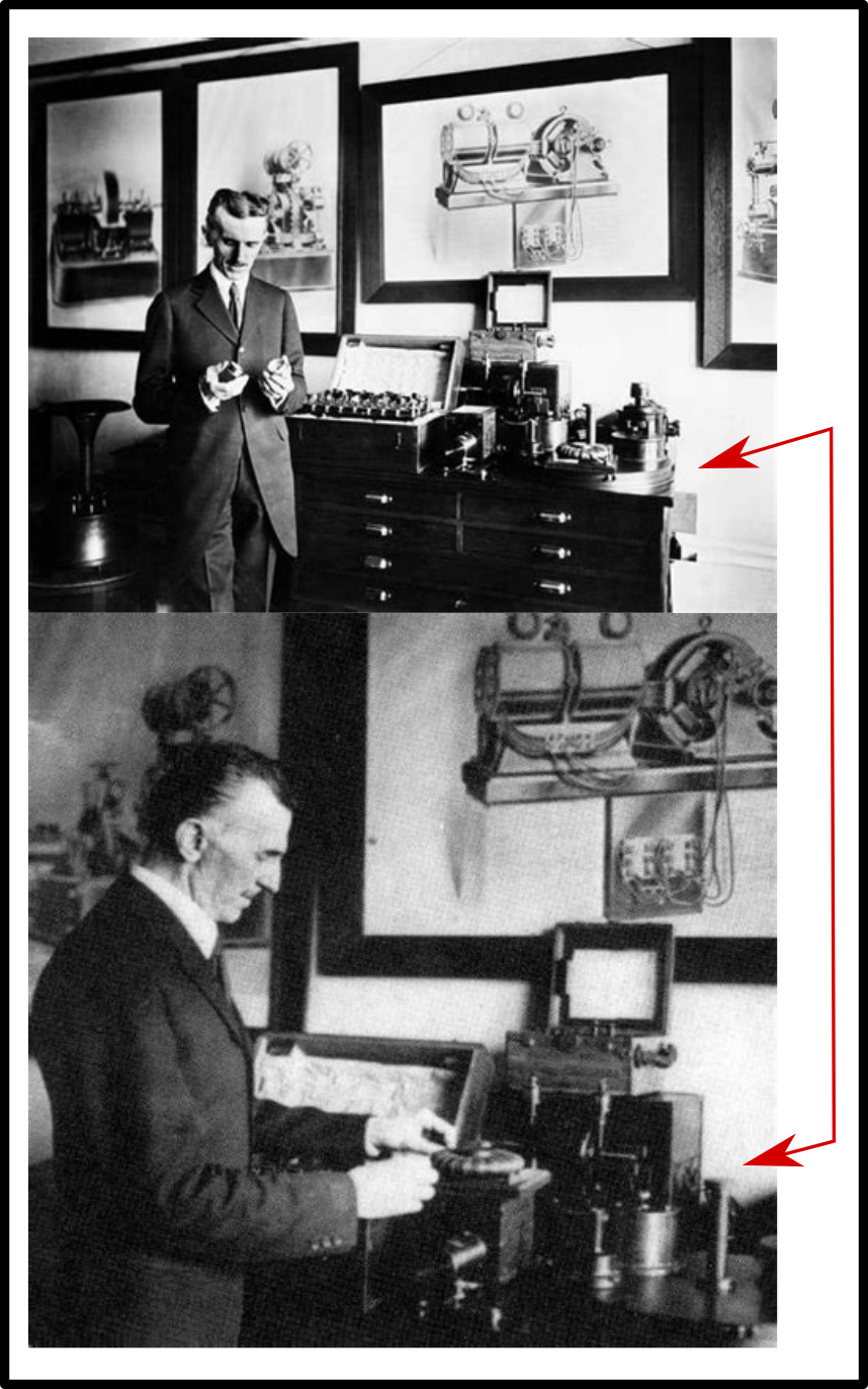
The exact parameters can be calculated and you can see by Tesla’s work in Colorado Springs, he realised that a short cylindrical coil can be better utilised than a long coil and a flat spiral is much more compact than any cylinder can be. These studies had revealed to Tesla a beautiful geometric design that cannot be improved any further, a very compact and portable unit that awaits a audience that has chosen to ignore his proclamations. Below is the coil I am talking about.
I have drawn up such a coil system, approx 400mm x 400mm x 200mm unit (approx), it unfolds and plugs into a power source (Tesla AC) and hopefully communicates to a clone at a preset short distance with losses. Not only voice/data but Energy as well (100 watts or so). The frequency was always too high to be of use in power transfer as the losses increased with the frequency.
Below are listed only my estimates by reading much data and personal experience.
Tesla system (no compromise).1 to 5…………………………..95 to 99
Radio system…………………………….99.9 to 100 0………………1 to 0.00001
High freq Tesla Flat……………………40……………………………….60
High freq Tesla Cyl……………………..60………………………………40
Low freq Tesla Flat…………………….15……………………………….85
Low freq Tesla Cyl……………………..30……………………………….70
So why did I design 336366 coil system using a traditional long cylinder? Simple, convenience and to prove to myself that the longitudinal velocity is the KEY to instant communication as Tesla suggested. Efficiency was not always the driving factor but the ease of material supply and a personal demand for longer wave lengths in a simple setup. The flat coil size became problematic in many ways, still I will go down that road again.
Coil…………………………………………………………..Volume and Area
Volume of Secondary………………………………0.0004 Cubic Mtrs
Surface Area of Secondary………………………0.796 Sqr Mtrs
MAX Volume of Primary…………………………..0.00068 Cubic Mtrs
MIN Volume of Primary……………………………0.000016 Cubic Mtrs
MAX Surface Area of Primary…………………..0.424 Sqr Mtrs
MIN Surface Area of Primary……………………0.01 Sqr Mtrs
Primary Volume at the design size…………..0.00045 Cubic Mtrs
Primary Surface Area at the design size…..0.285 Cubic Mtrs
What Turn…………………………………………………..14
What Area Secondary to Primary Equiv……..0.78 Sqr Mtrs
What Turn (beyond this design)…………………26
What Volume Secondary to Primary Equiv…0.0004 Cubic Mtrs
What Turn (very close )…………………………….13
I want to follow up with the real McCoy, in the not too distance future, regards Arto.
An error has occurred; the feed is probably down. Try again later.
Join 130 other subscribers
Published material Link
Talking to the Birds
Book Available NOW
At Amazon
At Createspace
https://www.createspace.com/4513692
______________________
Cartoons
http://www.scribd.com/doc/106684504/Scraps-Sketches-and-Satire
_______________________
Magic Square
http://www.scribd.com/doc/33050524/The-Magic-Square-of-Three-Crystal