When you are designing binary circuits you will need to display your results in Decimal so it readable by the user, such as Temperature, Distance and Arithmetic calculation results. There are 74LS chips that will make the conversion for you, such as the 74LS148. It seems like we need to investigate the Ternary version and see if reveals some interesting results.
1A
The first design (1A) utilises the well known Ternary TAND Gate, where the assertions are the positive voltage only.
1B
The second design (1B) replaces the TAND with a TONLY Gate as we have no need of the negative values if we are interfacing a binary circuit. Looking at the TONLY Gate it seems that we do not need such a complex gate as the ones used, maybe we could just use some Unary Gates to do the same job.
1C
Design (1C) fulfils this completely using only 3 Unary gates, by creating a USR Gate that can be modified by another input, in this case it is the positive that gets asserted from the result of the first input, the final Gate is just another cascade from the second Gate. The output is either positive or zero so it can be linked to a Binary circuit.
1D
The last design (1D) in this set reduces the Unary Gates to 2, thus allowing a negative as an output, this is mainly for use in other Ternary circuits, like the one I will show in another design (2B).
My basic approach to using Ternary, is to make it more useful than binary which has many short falls that nobody can see unless you have been involved in designing these circuits from scratch, the current pardigm requires a complex binary arch to acomplish results and requiring multiple iterations to arrive at a result. Where Ternary can accomplish more in less gate interations than binary. Each Ternary Gate is only slightly more complex than its Binary counterpart, such as the inverter.
These circuits show how much can be achieved with less resources while being less complex connections than the binary version.
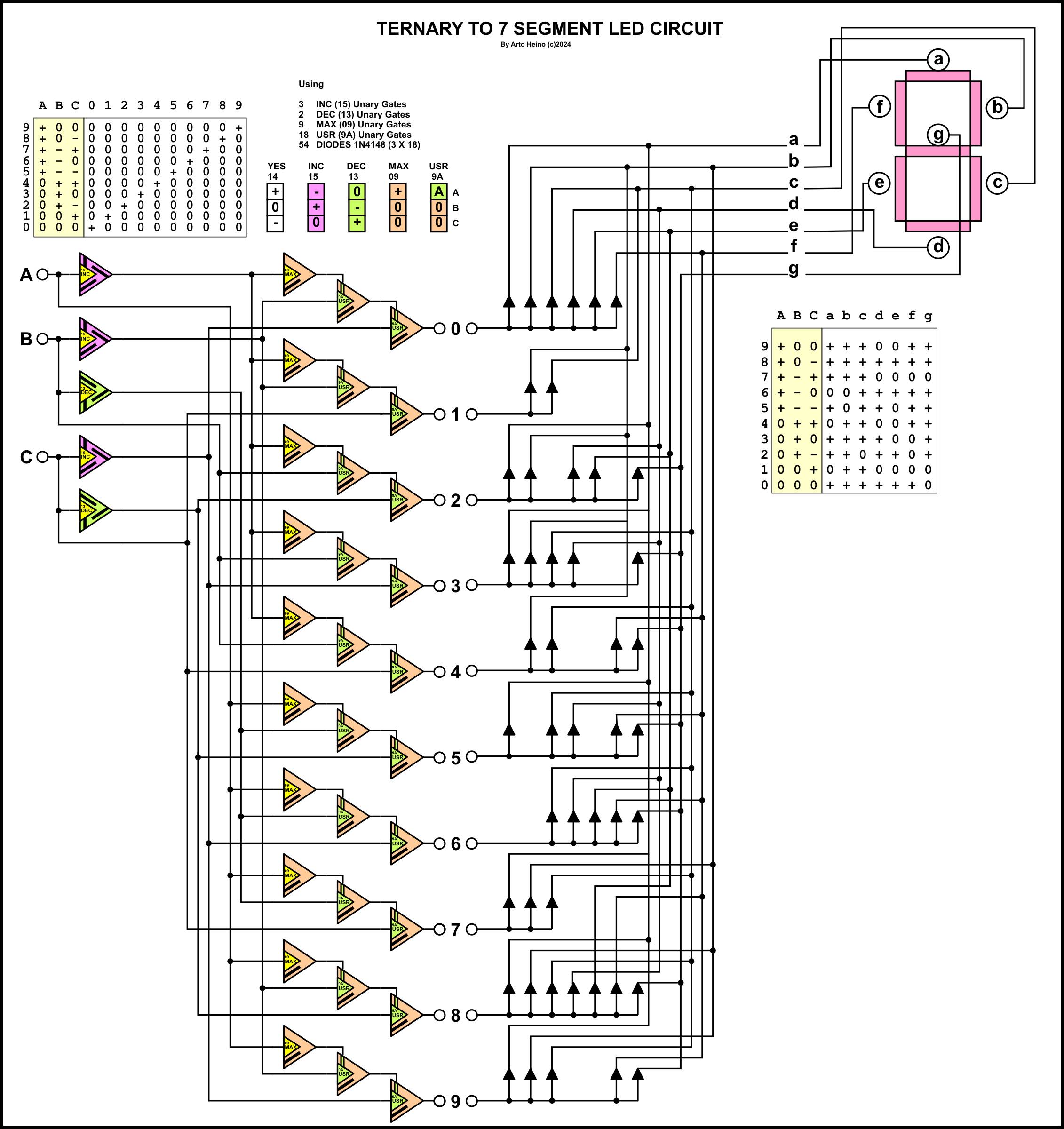
7 Segment Circuit
The final section is the Ternary to 7 Segment circuit. The first circuit (2A) is a basic 0 to 9 Led from a 3 Trit input, using the 3 Unary Gate logic from my earlier design (1C), the second circuit (2B) gives you another 9 more selections. Ternary easily uses negative numbers to increase data width selection, more elaborate schemes could be accomplished, like a complete 27 symbol choice, if I used all 13 positive numbers and all 13 negative numbers and zero.
2A
2B
Both of these designs use Diodes to accomplish the 7 Segment interface, making it suitable for a LED chip such as a Common Cathode TOS5121AR (Titan), LSD505400 (PlusOPTO), LTS-5003AWC (LITEON). You could even make your own with Leds or use a Large display.
I hope to finish my Division section of my Ternary ALU very soon, so far I have Addition, Subtraction, Multiply and a few Logic gates. I am still designing the shift registers and memory, while the ROM will be programmable with switches, I am basing it on 81 Trits at present.
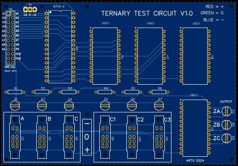
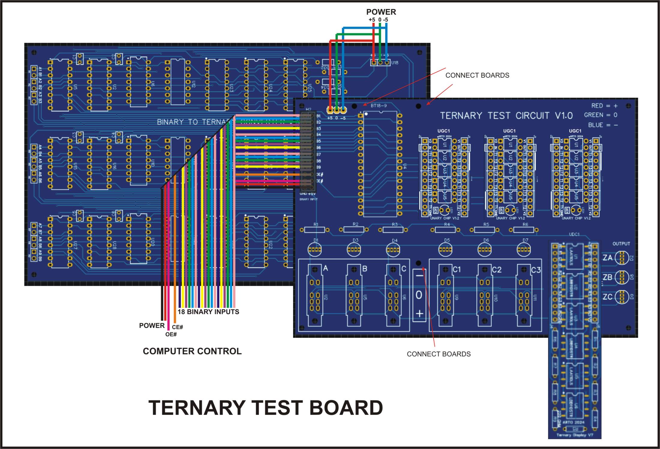
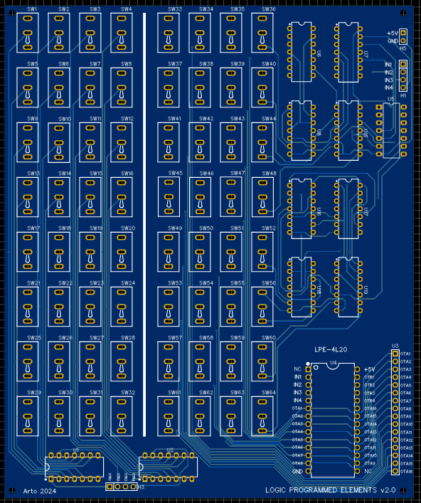
This board can accommodate 3 ternary chips the “BT18-9”, “UGC1” and “UDC1”, all of which are separate units, the BT18-9 needs either a set of ribbon cables with a socket or it can be directly connected with some HDR pins such as the connection diagram into the test board.
BT18-9
18 Binary paired Inputs (A1 B1) to (A9 B9) 9 Ternary outputs T0 to T8 OE# = output enable (you can set inputs then set to 0) CE# = chip enable (you must enable to 0 to start chip) +5V GND -5V
UGC1
1 Ternary input 1 Ternary output 1 led indictor of (-) 6 sets of programable inputs, in order
T1 T2 T3 T2 T3 T1 T3 T1 T2
T1 T3 T2 T2 T1 T3 T3 T3 T1
You can only connect 1 set at any one time, if you use a set of 3 jumper pins on all of the sets you could swap your combinations. These combinations will change your inputs into any one of six possibilities. This could also be done by using a analogue chip in a separate circuit.
UDC1
3 Ternary inputs 3 sets of 3 colour led outputs 3 sets of 3 colour led outputs (mirror of 1st set) So you could use these as Binary output switches or sensors as required. GND V1 = +5V V2 = spare 1 (-5v)
There are 3 ternary input switches (A B C) for all three RGB outputs (ZA ZB ZC) to function, there are also 3 selectors that need to be programmed first. Two of these are programmable by a binary source, while the other is by the onboard switches (C1 C2 C3). The current footprint of the display chip is 24pin pdip, even though the board is longer. As this is still only version 7, more work to do yet and I will eventually make it fit inside the boundary similar to the UGC1 board, on version 8 or 9. I am using optical relays in this design, something that I found useful in my ternary work.
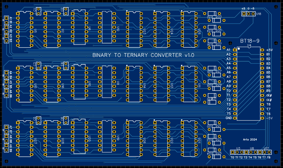
Starting from a Binary input where you have 2 bits to make a ternary trit:
00 = + 10 = 0 01 = –
The bit combination “11” is not valid and will not be used even though it is available as a binary output. The ternary converter ignores it.
Here are the 27 Unary gate combinations that are available and the binary combinations that will create them all. The UGI is the “Unary Gate Index”, numbering of all the gates in a system I have shown on my previous blogs.
Starting with the A1 and B1 as the first pair, then the A2,B2 then A3,B3, these three sets will give you a Unary set of 3 that will configure the basic Unary Chip “UGC1” to one of the 27 gates.
The second set A4,B4 + A5,B5 + A6,B6 will configure the next UGC1 gate. The third set are the switches C1,C2,C3 these will give you another UGC1 gate for you to use.
The outputs ZA,ZB,ZC correspond to the input data A,B,C, where your programmed UGC1 gate is being used to compute your result into the Z Led outputs. Where:
Red = + Green = 0 Blue = –
The input switches A,B,C,C1,C2,C3 also have RGB LEDs.
I hope this might start your interest in Ternary Logic and Computation, regards Arto.
** I have added UDC1 V8 to the Zipfile **
Ternary Test Boards PCB1D Zipfile
Al the PCB and Schematics for this project.
EasyEDA files only.
As a hobbyist I am always trying to work out how certain technologies function, so I decided to look into the PAL, PLA and any programmable logic arrays. So instead of using them as most technicians do I decided to create my own, by standard logic gates and switches, as I am just as interested in the why as the how.
These are my versions of Programmable Logic Arrays based on 74LS chips and 2 position toggle switches. I could try and replicate a standard PAL or PLE chip, but that would just clutter my simple approach as a learning tool. I made them so you can jumper the IC socket into to an existing circuit to test your programming.
LPA-4H10
Using AND/OR arrays, the AND array is either on(throughput) or off(made high) and the OR array is a fixed set to give you the maximum of multiple of outputs (6). My design is based on four 8 input AND gates, which are selectable by 8 switches, giving you a maximum of 32 switches. Using the 4 input bits and it’s inversion to give you 8 internal inputs for each AND gate.
IN1 x IN1# x IN2 x IN2# x IN3 x IN3# x IN4 x IN4# = OUTA1
Your input IN1 to IN4 are you only inputs, all the logic combinations are after your initial input.
AND Gates
2 INPUT, where A=INv and B=INw and Z=OUTAy (v = 1 to 4, w = 1 to 4, y = 1 to 4 )
AND NOT NOT AND AND AFBT ATBF NOR A B Z A# B Z A B# Z A# B# Z --------- --------- --------- --------- 0 0 0 1 0 0 0 1 0 1 1 1 0 1 0 1 1 1 0 0 0 1 0 0 1 0 0 0 0 0 1 1 1 0 1 0 1 1 1 0 1 0 1 0 0 0 0 0
3 INPUT
A B C Z A# B C Z A B# C Z A B C# Z ------------------ 0 0 0 0 0 0 1 0 0 1 0 0 0 1 1 0 1 1 1 1 1 0 0 0 1 0 1 0 1 1 1 1 1 1 0 0 1 1 1 1 1 1 1 1
A B# C# Z A# B# C Z A# B C# Z A# B# C# Z ------------------ 0 1 1 0 1 1 1 1 0 1 0 0 1 1 1 1 0 0 1 0 1 1 1 1 0 0 0 0 1 1 1 1 1 1 0 0 1 0 1 0 1 0 0 0
The abbreviations AFBT and ATBF was devised by me to simplify some of the less known logic gates that are available to the binary combinations. All these odd types of gates can be created with AND, OR, XOR, NOR, XNOR or NAND gates with an inverter on one of the gates as well. I don’t know how useful my ideas are to those Engineers who were educated in Digital Logic, but as an intuitive tool that I have developed, it has given me an insight into applying digital Systems to my Ternary work. As Ternary logic has a massive (19683) number of 2 input elements, your mind boggles at the idea of “Truelean Logic” as opposed to “Boolean Logic” which has only 16 two input elements. Here is the Matrix I developed when I sorted my relay logic elements, it clearly shows how it was developed.
AFBT (AfBt)
Z = (A = False = 0) + (B = True = 1) = True = 1 Z only equals True when (A = False = 0) and (B = true = 1) all the rest are False = 0. If you look at the A input as inverted you will have the same as standard logic, as such:
My Symbol: ____ A ----\ \ | \---------- Z B ----/____|
De Morgans Symbol2 Gated Logic _____ _____ A ----O| \ A ---|>O--| \ | |------- Z = | |--- Z B -----|_____/ B --------|_____/
ATBF (AtBf)
Z = (A = True = 1) + (B = False = 0) = True = 1 Z only equals True when (A = True = 1) and (B = False = 0) all the rest are False = 0. If you look at the B input as inverted you will have the same as standard logic, as such:
My Symbol: _____ A ----\ | | /---------- Z B ----/___/
De Morgans Symbol2 Gated Logic _____ _____ A -----| \ A --------| \ | |------- Z = | |------ Z B ----O|_____/ B ---|>O--|_____/
My Symbolism for multiple inputs
AfBCDEFGt

           *     *     *     *     *     *
Z = (A=0)+(B=1)+(C=1)+(D=1)+(E=1)+(F=1)+(G=1)=1

ACDEFGtBf

     *           *     *     *     *     *
Z = (A=1)+(B=0)+(C=1)+(D=1)+(E=1)+(F=1)+(G=1)=1

ABDFGtCEf

     *     *           *           *     *
Z = (A=1)+(B=1)+(C=0)+(D=1)+(E=0)+(F=1)+(G=1)=1
LPA Logic
The output from the AND array goes into a OR array that is set by 2 inputs using a OR combination, such as:
As you can see there are no more possible combinations than these six for a 2 input OR gate. Another added output is the ANDed output before the ORing which gives you another 4 outputs to use, giving you a total of 10 outputs.
Example 1a:
Here are the equations you can use, by using only IN1 and IN2 as your inputs:
So if you use two inputs, also using only 2 switchs F1 ans F2 of both inputs. Thus you get:
“#” = inversion
“^” = high = 1 (off)
OUTR1 = ((IN1 x F1) x (IN1# x F2^)) + ((IN2 x F1^) x (IN2# x F2))
When a switch “F” is on, then it equals the “IN” input. If “F” if off the it is high (=1).
If, IN1 = 1/0 and F1 is on and F2 is off (1), the rest of the switches are off (1) IN1(F3-F8). Every even switch uses the inverted version of the odd input going to the internal OR inputs.
also, IN2 = 1/0 and F1 is off (1) and F1 is on, the rest of the switches will be off (1) IN2(F3-F8)
IN1(F2) IN2(F1) = switch to high
             AND				OR
             _____
IN1 -0101---|  F1 \  	0101	             ______
            |      |------- OUTA1 ---0101 ---\      \
IN1 -0101--O|__F2_/ 	1111	              |      \
                                              |       \__OUTR1_1101
             _____		              |       /
IN2 -0110---|  F1 \  	1111	              |      /
            |      |------- OUTA2 ---1001 ---/______/
IN2 -0110--O|__F2_/ 	1001
This will give you output to the OUTR1 line, the OUTA1 and OUTA2. This is the output when you swutch IN1(F2) and IN2(F1) to high;
If IN1 = 0 and IN2 = 0 then OUTR1 = 1 , OUTA1 = 0 , OUTA2 = 1 If IN1 = 1 and IN2 = 0 then OUTR1 = 1 , OUTA1 = 1 , OUTA2 = 1 If IN1 = 0 and IN2 = 1 then OUTR1 = 0 , OUTA1 = 0 , OUTA2 = 0 If IN1 = 1 and IN2 = 1 then OUTR1 = 1 , OUTA1 = 1 , OUTA2 = 0
Where switch position “on” allows your input to go through the circuit, while “off” is only “high” (1) so the AND gate now is one less than your total maximum of 8. So if you switch all 8 to “off” this input will be only be a “1”, giving you a “1” on the input to one of the set OR matrix inputs.
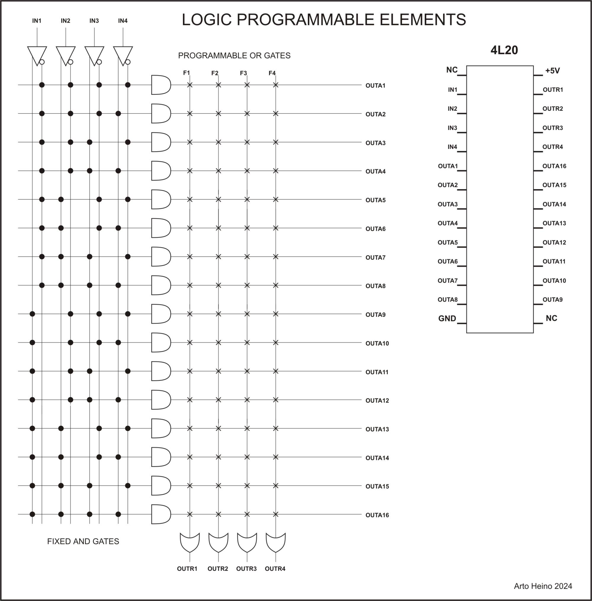
LPE-4L20
You get 4 inputs plus its internal inversions giving you 4 outputs (ORed) and 16 AND combinations. The off switch position is low, thus negating it throughput.
X = input o = inverted input
My first AND Matrix;
1 2 3 4 5 6 7 8 9 1 1 1 1 1 1 1
                  0 1 2 3 4 5 6
x x x x . x x . x . . x . . . .
. . . . o . . o . o o . o o o o

x x x . x x . . . x x . x . . .
. . . o . . o o o . . o . o o o

x x . x x . . x x . x . . x . .
. . o . . o o . . o . o o . o o

x . x x x . x x . x . . . . x .
. o . . . o . . o . o o o o . o
I was going to use this internal format, until I decided to use the standard PLE arrangement.
--------------------------------
   |   |   |   |   |   |   |
1 2 3 4 5 6 7 8 9 1 1 1 1 1 1 1		Net     AND Inverter output
                  0 1 2 3 4 5 6
. . . . . . . . x x x x x x x x   	H1  	A   1A
o o o o o o o o . . . . . . . .		U5_2	    1Y

. . . . x x x x . . . . x x x x 	H2	B   2A
o o o o . . . . o o o o . . . .		U5_4	    2Y

. . x x . . x x . . x x . . x x 	H3	C   3A
o o . . o o . . o o . . o o . .		U5_6	    3Y

. x . x . x . x . x . x . x . x		H4	D   4A
o . o . o . o . o . o . o . o .		U5_8	    4Y
So if you want to implement a 4 input XOR gate:
FnXOR = XOR (IN1 IN1# IN2 IN2# IN3 IN3# IN4 IN4#)
 =
(IN1 X IN2# X IN3# X IN4#) +
(IN1# X IN2 X IN3# X IN4#) +
(IN1# X IN2# X IN3 X IN4#) +
(IN1# X IN2# X IN3# X IN4) +
(IN1 X IN2 X IN3 X IN4#) +
(IN1 X IN2 X IN3# X IN4) +
(IN1 X IN2# X IN3 X IN4) +
(IN1# X IN2 X IN3 X IN4)
Switches used: (from 1 to 64) 5 9 17 29 33 45 53 57 – or – first column (1 to 16) 2 3 5 8 9 12 14 15 are ON all other switches are OFF
“Talking to the Birds”, by Arto Juhani Heino, Volume I, is now available on Amazon.com, 12 Chapters, 356 pages over 250 illustrations and over 70 charts. A diverse compilation of essays, studies and illustrations in the underlying designs and principles behind some of the Arts, Sciences and with some social commentary, taken from an Artists perspective on the world he studies. A book where Art, Engineering and the ancient world meet. Highly illustrated , with artwork, numeric tables, geometries, designs and schematics. It has sections on Tesla, Hendershot, Don Smith, Moray, Sixto Ramos and Ucros. This is Volume I, Volume II is being complied at present.
Here is a pictures that shows some of the backlog in hand written books waiting to be converted to material for next couple of volumes.
I would like to thank all my readers and those who have helped me to bring my work to the public, I am working hard on the next couple of volumes. Watch my blog for some interesting new articles. Regards Arto.
An error has occurred; the feed is probably down. Try again later.
Join 130 other subscribers
Published material Link
Talking to the Birds
Book Available NOW
At Amazon
At Createspace
https://www.createspace.com/4513692
______________________
Cartoons
http://www.scribd.com/doc/106684504/Scraps-Sketches-and-Satire
_______________________
Magic Square
http://www.scribd.com/doc/33050524/The-Magic-Square-of-Three-Crystal