When you are designing binary circuits you will need to display your results in Decimal so it readable by the user, such as Temperature, Distance and Arithmetic calculation results. There are 74LS chips that will make the conversion for you, such as the 74LS148. It seems like we need to investigate the Ternary version and see if reveals some interesting results.
1A
The first design (1A) utilises the well known Ternary TAND Gate, where the assertions are the positive voltage only.
1B
The second design (1B) replaces the TAND with a TONLY Gate as we have no need of the negative values if we are interfacing a binary circuit. Looking at the TONLY Gate it seems that we do not need such a complex gate as the ones used, maybe we could just use some Unary Gates to do the same job.
1C
Design (1C) fulfils this completely using only 3 Unary gates, by creating a USR Gate that can be modified by another input, in this case it is the positive that gets asserted from the result of the first input, the final Gate is just another cascade from the second Gate. The output is either positive or zero so it can be linked to a Binary circuit.
1D
The last design (1D) in this set reduces the Unary Gates to 2, thus allowing a negative as an output, this is mainly for use in other Ternary circuits, like the one I will show in another design (2B).
My basic approach to using Ternary, is to make it more useful than binary which has many short falls that nobody can see unless you have been involved in designing these circuits from scratch, the current pardigm requires a complex binary arch to acomplish results and requiring multiple iterations to arrive at a result. Where Ternary can accomplish more in less gate interations than binary. Each Ternary Gate is only slightly more complex than its Binary counterpart, such as the inverter.
These circuits show how much can be achieved with less resources while being less complex connections than the binary version.
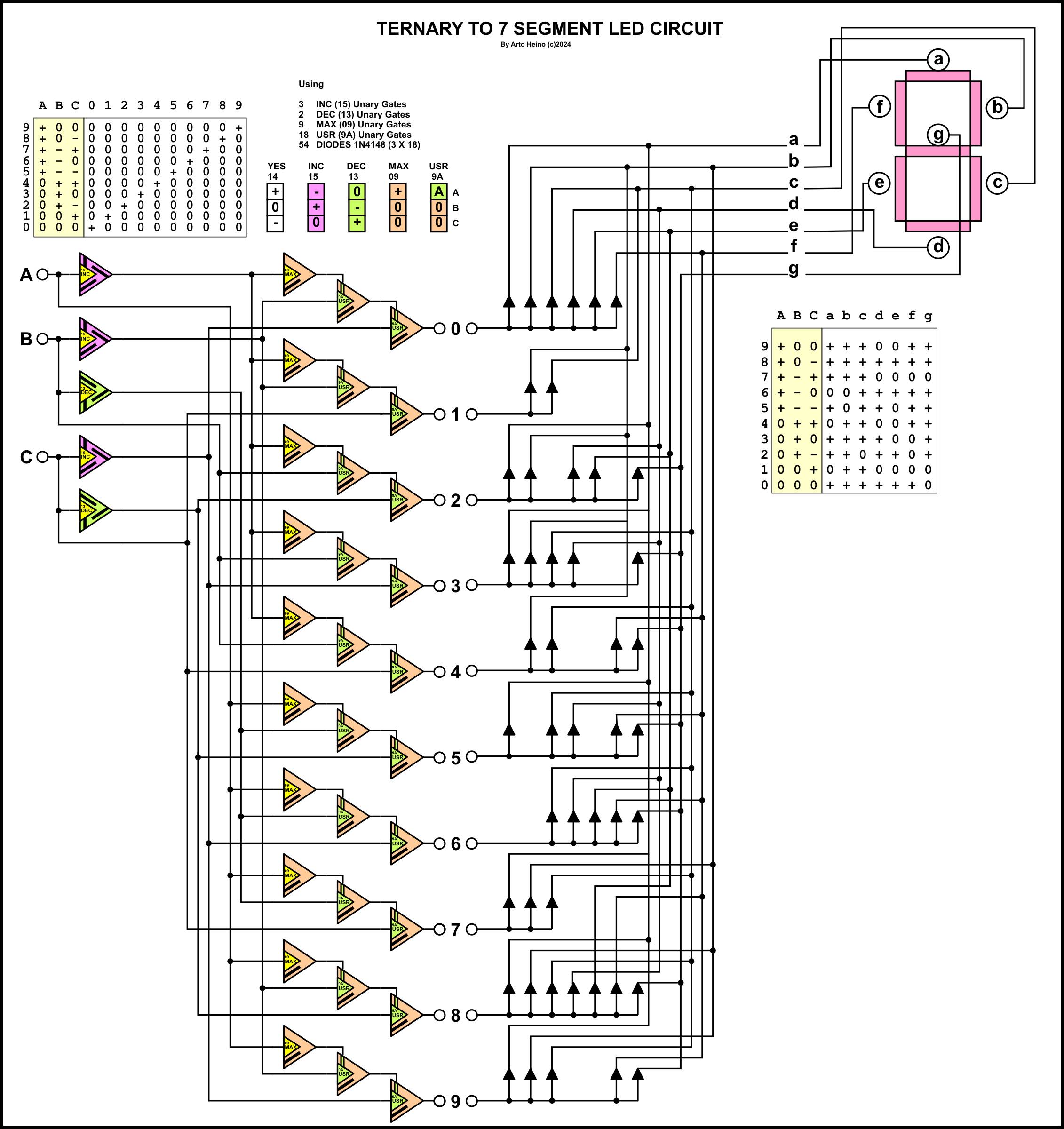
7 Segment Circuit
The final section is the Ternary to 7 Segment circuit. The first circuit (2A) is a basic 0 to 9 Led from a 3 Trit input, using the 3 Unary Gate logic from my earlier design (1C), the second circuit (2B) gives you another 9 more selections. Ternary easily uses negative numbers to increase data width selection, more elaborate schemes could be accomplished, like a complete 27 symbol choice, if I used all 13 positive numbers and all 13 negative numbers and zero.
2A
2B
Both of these designs use Diodes to accomplish the 7 Segment interface, making it suitable for a LED chip such as a Common Cathode TOS5121AR (Titan), LSD505400 (PlusOPTO), LTS-5003AWC (LITEON). You could even make your own with Leds or use a Large display.
I hope to finish my Division section of my Ternary ALU very soon, so far I have Addition, Subtraction, Multiply and a few Logic gates. I am still designing the shift registers and memory, while the ROM will be programmable with switches, I am basing it on 81 Trits at present.
As a hobbyist I am always trying to work out how certain technologies function, so I decided to look into the PAL, PLA and any programmable logic arrays. So instead of using them as most technicians do I decided to create my own, by standard logic gates and switches, as I am just as interested in the why as the how.
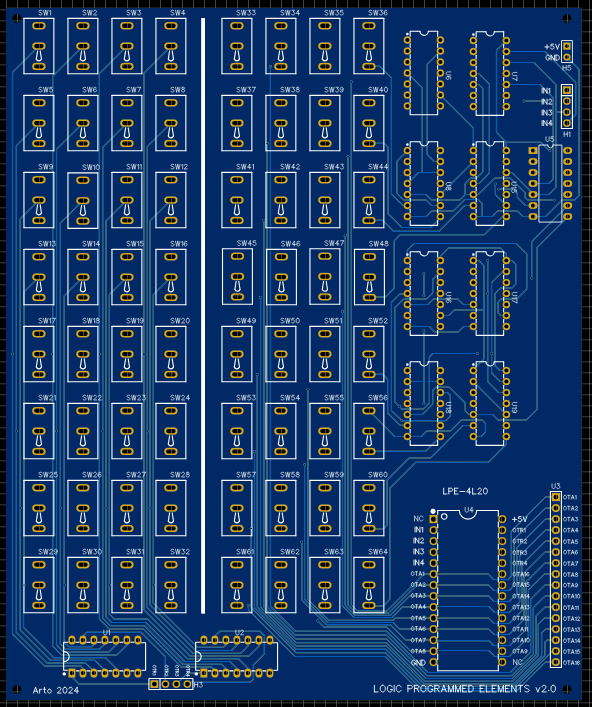
These are my versions of Programmable Logic Arrays based on 74LS chips and 2 position toggle switches. I could try and replicate a standard PAL or PLE chip, but that would just clutter my simple approach as a learning tool. I made them so you can jumper the IC socket into to an existing circuit to test your programming.
LPA-4H10
Using AND/OR arrays, the AND array is either on(throughput) or off(made high) and the OR array is a fixed set to give you the maximum of multiple of outputs (6). My design is based on four 8 input AND gates, which are selectable by 8 switches, giving you a maximum of 32 switches. Using the 4 input bits and it’s inversion to give you 8 internal inputs for each AND gate.
IN1 x IN1# x IN2 x IN2# x IN3 x IN3# x IN4 x IN4# = OUTA1
Your input IN1 to IN4 are you only inputs, all the logic combinations are after your initial input.
AND Gates
2 INPUT, where A=INv and B=INw and Z=OUTAy (v = 1 to 4, w = 1 to 4, y = 1 to 4 )
AND NOT NOT AND AND AFBT ATBF NOR A B Z A# B Z A B# Z A# B# Z --------- --------- --------- --------- 0 0 0 1 0 0 0 1 0 1 1 1 0 1 0 1 1 1 0 0 0 1 0 0 1 0 0 0 0 0 1 1 1 0 1 0 1 1 1 0 1 0 1 0 0 0 0 0
3 INPUT
A B C Z A# B C Z A B# C Z A B C# Z ------------------ 0 0 0 0 0 0 1 0 0 1 0 0 0 1 1 0 1 1 1 1 1 0 0 0 1 0 1 0 1 1 1 1 1 1 0 0 1 1 1 1 1 1 1 1
A B# C# Z A# B# C Z A# B C# Z A# B# C# Z ------------------ 0 1 1 0 1 1 1 1 0 1 0 0 1 1 1 1 0 0 1 0 1 1 1 1 0 0 0 0 1 1 1 1 1 1 0 0 1 0 1 0 1 0 0 0
The abbreviations AFBT and ATBF was devised by me to simplify some of the less known logic gates that are available to the binary combinations. All these odd types of gates can be created with AND, OR, XOR, NOR, XNOR or NAND gates with an inverter on one of the gates as well. I don’t know how useful my ideas are to those Engineers who were educated in Digital Logic, but as an intuitive tool that I have developed, it has given me an insight into applying digital Systems to my Ternary work. As Ternary logic has a massive (19683) number of 2 input elements, your mind boggles at the idea of “Truelean Logic” as opposed to “Boolean Logic” which has only 16 two input elements. Here is the Matrix I developed when I sorted my relay logic elements, it clearly shows how it was developed.
AFBT (AfBt)
Z = (A = False = 0) + (B = True = 1) = True = 1 Z only equals True when (A = False = 0) and (B = true = 1) all the rest are False = 0. If you look at the A input as inverted you will have the same as standard logic, as such:
My Symbol: ____ A ----\ \ | \---------- Z B ----/____|
De Morgans Symbol2 Gated Logic _____ _____ A ----O| \ A ---|>O--| \ | |------- Z = | |--- Z B -----|_____/ B --------|_____/
ATBF (AtBf)
Z = (A = True = 1) + (B = False = 0) = True = 1 Z only equals True when (A = True = 1) and (B = False = 0) all the rest are False = 0. If you look at the B input as inverted you will have the same as standard logic, as such:
My Symbol: _____ A ----\ | | /---------- Z B ----/___/
De Morgans Symbol2 Gated Logic _____ _____ A -----| \ A --------| \ | |------- Z = | |------ Z B ----O|_____/ B ---|>O--|_____/
My Symbolism for multiple inputs
AfBCDEFGt

           *     *     *     *     *     *
Z = (A=0)+(B=1)+(C=1)+(D=1)+(E=1)+(F=1)+(G=1)=1

ACDEFGtBf

     *           *     *     *     *     *
Z = (A=1)+(B=0)+(C=1)+(D=1)+(E=1)+(F=1)+(G=1)=1

ABDFGtCEf

     *     *           *           *     *
Z = (A=1)+(B=1)+(C=0)+(D=1)+(E=0)+(F=1)+(G=1)=1
LPA Logic
The output from the AND array goes into a OR array that is set by 2 inputs using a OR combination, such as:
As you can see there are no more possible combinations than these six for a 2 input OR gate. Another added output is the ANDed output before the ORing which gives you another 4 outputs to use, giving you a total of 10 outputs.
Example 1a:
Here are the equations you can use, by using only IN1 and IN2 as your inputs:
So if you use two inputs, also using only 2 switchs F1 ans F2 of both inputs. Thus you get:
“#” = inversion
“^” = high = 1 (off)
OUTR1 = ((IN1 x F1) x (IN1# x F2^)) + ((IN2 x F1^) x (IN2# x F2))
When a switch “F” is on, then it equals the “IN” input. If “F” if off the it is high (=1).
If, IN1 = 1/0 and F1 is on and F2 is off (1), the rest of the switches are off (1) IN1(F3-F8). Every even switch uses the inverted version of the odd input going to the internal OR inputs.
also, IN2 = 1/0 and F1 is off (1) and F1 is on, the rest of the switches will be off (1) IN2(F3-F8)
IN1(F2) IN2(F1) = switch to high
             AND				OR
             _____
IN1 -0101---|  F1 \  	0101	             ______
            |      |------- OUTA1 ---0101 ---\      \
IN1 -0101--O|__F2_/ 	1111	              |      \
                                              |       \__OUTR1_1101
             _____		              |       /
IN2 -0110---|  F1 \  	1111	              |      /
            |      |------- OUTA2 ---1001 ---/______/
IN2 -0110--O|__F2_/ 	1001
This will give you output to the OUTR1 line, the OUTA1 and OUTA2. This is the output when you swutch IN1(F2) and IN2(F1) to high;
If IN1 = 0 and IN2 = 0 then OUTR1 = 1 , OUTA1 = 0 , OUTA2 = 1 If IN1 = 1 and IN2 = 0 then OUTR1 = 1 , OUTA1 = 1 , OUTA2 = 1 If IN1 = 0 and IN2 = 1 then OUTR1 = 0 , OUTA1 = 0 , OUTA2 = 0 If IN1 = 1 and IN2 = 1 then OUTR1 = 1 , OUTA1 = 1 , OUTA2 = 0
Where switch position “on” allows your input to go through the circuit, while “off” is only “high” (1) so the AND gate now is one less than your total maximum of 8. So if you switch all 8 to “off” this input will be only be a “1”, giving you a “1” on the input to one of the set OR matrix inputs.
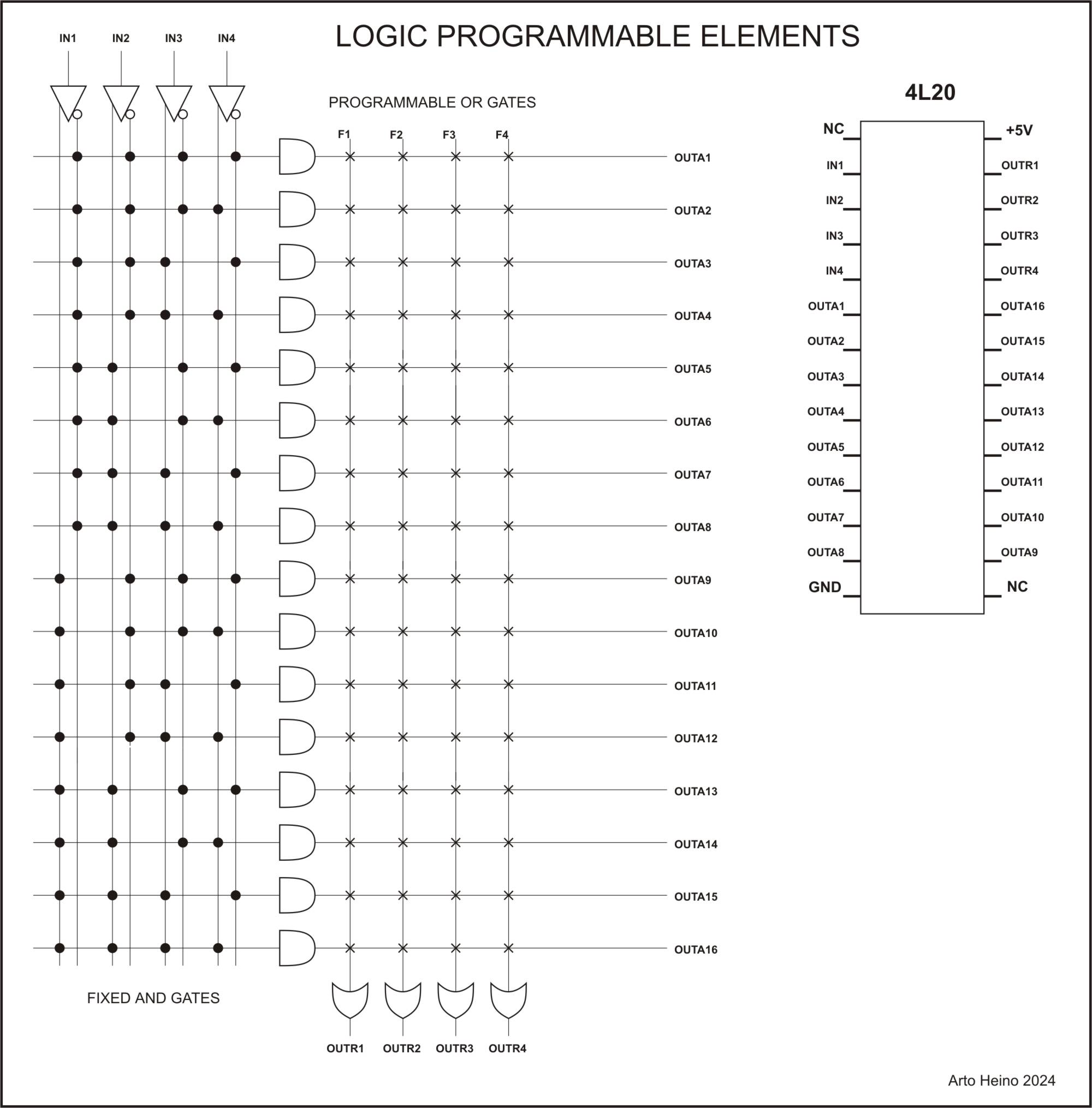
LPE-4L20
You get 4 inputs plus its internal inversions giving you 4 outputs (ORed) and 16 AND combinations. The off switch position is low, thus negating it throughput.
X = input o = inverted input
My first AND Matrix;
1 2 3 4 5 6 7 8 9 1 1 1 1 1 1 1
                  0 1 2 3 4 5 6
x x x x . x x . x . . x . . . .
. . . . o . . o . o o . o o o o

x x x . x x . . . x x . x . . .
. . . o . . o o o . . o . o o o

x x . x x . . x x . x . . x . .
. . o . . o o . . o . o o . o o

x . x x x . x x . x . . . . x .
. o . . . o . . o . o o o o . o
I was going to use this internal format, until I decided to use the standard PLE arrangement.
--------------------------------
   |   |   |   |   |   |   |
1 2 3 4 5 6 7 8 9 1 1 1 1 1 1 1		Net     AND Inverter output
                  0 1 2 3 4 5 6
. . . . . . . . x x x x x x x x   	H1  	A   1A
o o o o o o o o . . . . . . . .		U5_2	    1Y

. . . . x x x x . . . . x x x x 	H2	B   2A
o o o o . . . . o o o o . . . .		U5_4	    2Y

. . x x . . x x . . x x . . x x 	H3	C   3A
o o . . o o . . o o . . o o . .		U5_6	    3Y

. x . x . x . x . x . x . x . x		H4	D   4A
o . o . o . o . o . o . o . o .		U5_8	    4Y
So if you want to implement a 4 input XOR gate:
FnXOR = XOR (IN1 IN1# IN2 IN2# IN3 IN3# IN4 IN4#)
 =
(IN1 X IN2# X IN3# X IN4#) +
(IN1# X IN2 X IN3# X IN4#) +
(IN1# X IN2# X IN3 X IN4#) +
(IN1# X IN2# X IN3# X IN4) +
(IN1 X IN2 X IN3 X IN4#) +
(IN1 X IN2 X IN3# X IN4) +
(IN1 X IN2# X IN3 X IN4) +
(IN1# X IN2 X IN3 X IN4)
Switches used: (from 1 to 64) 5 9 17 29 33 45 53 57 – or – first column (1 to 16) 2 3 5 8 9 12 14 15 are ON all other switches are OFF
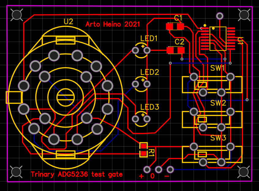
Rather than try to instigate the trinary action directly from the positive, neutral and negative charges, I have simplified it by setting the switches using only the positive rail and neutral before I have set the Unary Gates, using a ADG5236 Analog switch chip. This is only a testing measure to get all the gates ready for integration into combinatory sets like Tand and Tnor. You can say combinatory only in Ternary because each two input gate is made up of three Unary gates from a pool of 27, while each Unary gates is made up of three switched sets, sometimes as two pairs of DPDT while one is redundant, due to the lack of physical trinary switches available on the market.
I have tried not to compromise on either side of the switched in/out design, still we need to move these ideas forward so we can find interesting and valuable Ternary circuits that can accomplish much and more of what its little Binary brother has done in the last 80 years. The use of CMOS, PMOS, NMOS have been used successfully by many inventors to create Trinary circuits but have never been popularised due to the logical tangle of the unknown element “0”. This by philosophical terms is the “unknown”, “undefined” or “undecided” element, as binary has either Yes or No to which there is an easy determinate path to follow, no questions about a vague unknown.
This dilemma of the neutral place where indecision is its home, is merely an illusion that has been created by a physiological inability of our mind to see it any other way. I offer a simpler approach where S. C. Kleene, Post, Lukasiewicz and others has written much on the mathematics and semantics of this, where as I see it as a natural condition of our physical universe. The Earth is the simple model I follow, where the positive charges are above us and the negative charges are below us, while we stand on the neutral ground. This simple model also works for water and any other boundary situation where “0” is now the path of all connections made by its very nature, a skin if you like. (as above a mirror as it is below). Indecision is not unknown, it can be weighed just as gravity can be defined by units being weighed, a heavy object as opposed to a light one.
Much has been written about mathematics of ternary and it has its advantages over binary for sure, here is some simple arithmetic. Again I follow my simple model:
There is a simple and enduring beauty using trinary logistics, you never end up in a lock up situation, due to the neutral line where it can always carry its logic to a complete solution. The binary has the problem of only having a “true” and “false” narrative, where that is not how nature works at all.
The early Atomic physicists had to resort to phantoms of matter such as “Electrons”, “Neutrons” and “Protons”, these are mere conventions of usage not a reality of our universe. They used these mnemonic devices to solve abstractions they did not fully comprehend. Charge is all we really know, sadly the Ether was incorrectly dismissed in the 20th Century as the carrier of all the physical universe, not so, as we should simply state that charge is one of the different conditions of the Ether. This also makes the Ether as a neutral state, thus making it the default condition of everything that is not moving, or charged in any way, while Gravity is the Pressure of the Ether on all Mass.
Once Trinary thought is used in all circumstances, War, Famine, Invention and Mans ailing conditions will improve beyond mere Utopian dreams. False narratives and political agendas will be nothing but illusions we will all see through and will serve no purpose in our pursuit of our quality of life and living. The Us and Them syndrome are but Marxist drivel used to divide our sensibilities against the true knowledge of our existence.
Trinary thinking no longer separates us into “Right” and “Wrong”, “True” and False”, “Yes” and “No” but introduces gradations of wisdom and experience. I ask is it wrong that a bird can walk while it is only known to fly in the minds of many. Is the colour of the sky Blue when we see it as Red, Orange and Yellow at other times. Binary thinking divides our perceptions along a boundary, this boundary is the “Undecided” or Neutral line which we will now understand in Trinary thought, as the connector of everything. In electrical engineering it has always been called “Earth”, “Common” or “Neutral”.
Art precedes science just as culture precedes politics, this is why “reductio ad absurdum” of modern philosophy is a regressive step with the binary decision trees built from notions of “Left” and “Right” factions are nonsense and are a danger to our own survival. The Quantum arguments currently exploited by “Modern Science” are but Binary semantics made into a religion, called “Scientism”. The rulers of our lives only require serfs not thinking individuals, who have, graduations of thought and experience where true diversity only exists when we are allowed to think freely.
Addition of Trinary
+ add + = +-
which is
1 + 1 = 2
+- add +- = ++
which is
2 + 2 = 4
so if “-” = -1
then
– add – = -+
which is
-1 + -1 = -2
Try
-1 + 1 = 0 or 1 – 1 = 0
which is
– add + = 0
So a balanced ternary system is similar to the way we use electrical charge as well.
Here are the diagrams from my work, it will be included in my next volume “Talking To The Birds, Volume II”, coming soon, regards Arto.
From my last entry I hinted at a 555 relay emulation, I am not quite their yet, I am getting close though. Here is my current stage I am on at the present moment.
I needed an ALU to start things of, so I started on the Half-Adder as a building block, here is my iterations.
The next step is the Full-Adder and its first few iterations from Logic Gates.
Lastly I have included a simple idea of how some of these could be interpreted in the 3D world, more to come on this aspect in a future blog.
If your response is high enough, I will start a Patreon account and begin building the real thing, regards Arto.
It looks like I am reinventing the wheel, minus valves and transistors, this work might even seem redundant to some of the techno-nerds. I assure you this is a step forward, there has been no time in the last 50 years that all those electronic enthusiasts have been able to simplify and create something without an official corporately designed IC package doing all your brain-work for you, leaving nothing for your own original imagination. I was very excited many years ago when many hobbyists made their own computers from discreet transistors and IC packages, while a few even made some relay ALUs.
While I thought of making my own CPU from relays but resisted, I first needed to create a new architecture that could incorporate an open 256 bit CPU and a Analog CPU in one package, while still accessible enough to be built by hand. This was part of my goal, as the architecture had to be robust, to last 1000 years, the components were to be the built environment and the power to drive it should be available 24/7, sounds like a pipe dream of some mad scientist. I only dare to dream of its reality and decided to rediscover the simplicity and the basic technology to make it plausible. The idea of using stone to contain the complex logical matrix that can be accessed via simple interfaces is the final reality, the many steps to arrive at that outcome might outstrip my lifetime, still I will persist, as I cannot dismiss a vision that is clear and within the realms of possibility.
Enough of my machinations, here are some interesting and practically solved devolutions of known devices from my last posting. Here is a FlipFlop made from two relay NAND gates.
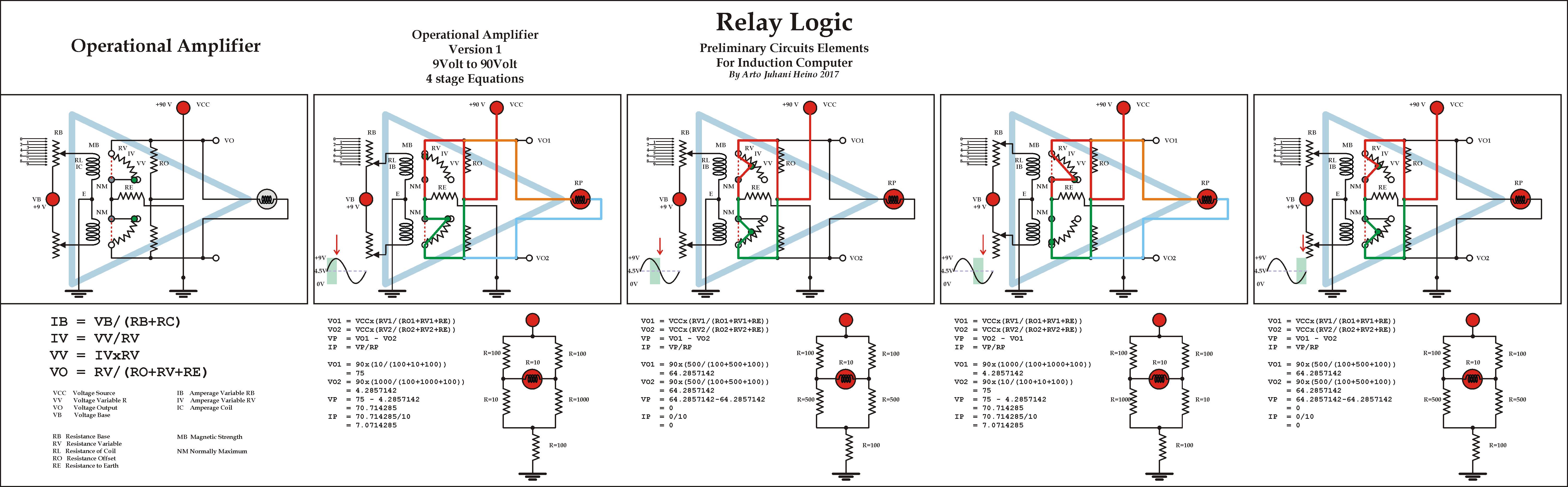
While the idea of a Operational Amplifier kept me awake for a night of two, I hope to emulate a 555 IC chip from my work here, just in time to compete a chapter in my Volume II.
This version should satisfy many of its Integrated Chip operations, still it is a crude and very fundamental design, useful to be expanded upon with a bit more work. I must repeat, I am not an electrical engineer and I have no degree from any University, I am truly a ground up natural scientist, where my tenets of understanding come from a life time of artistic creativity with careful observations and practical applications. I hope those who are interested can learn much from my ideas. Regards Arto.
Here are some interesting combinations using relays as logic gates, which was where I began this first step into the Induction Computer.
As you can see I have “single relays” and “double pole relays” and “Latch relays”, an old technology that goes back to the beginnings of the study of electromagnetism in the 1800’s. My studies into remnant magnetism of different materials, brought me into an understanding of natural rocks and the possibility of using either “Granite”, other rocks or even a poured casting as a magnetically imprinted “Logic Matrix Array”, storing functions, complex procedures, information and even pictures, videos and music.
In the Voltage Multiplier I have even eliminated any semiconductors, even diodes and batteries, while only using coils, capacitors, magnets and relay operations. You can see my process of elimination and the final schematic being without any high tech micro components.
There are a few parts to make the whole system function, here are some of the descriptions for the Voltage Multiplier.
The Slab that must have
1 Remnant Magnetism within permissible limits
2 Flat Surface, possibly engraved for descriptive and functional reasoning
3 Location keys for Imprinter and Reader
The Matrix Imprinter
1 Magnetic Array
2 Electromagnetic Array
3 Reset and Wipe function
The Induction Reader
1 Layered Switch Array
2 Geometric Coil Matrix
3 External Switches/Buttons and Levers/Handles arced or rotary
Physical Actions of Operator
1 Generate Voltage
2 Instigate Switch Operations
3 Discharge to external device
As this blog article is only to describe some of my work, it is not the whole article, that you will find in my next volume of “Talking To The Birds” Volume II. If the interest in these ideas are popular, I would consider a FundMe or Patreon profile and begin the arduous progress of a working system , regards Arto.
My invention(AMOD) is now 10 years old to me, I have waited for the IBM, Sony, Hitachi, etc to come up with the solution of CD and DVD spin reliability and to eventually supersede it to a simpler more efficient solution, as usual they are making too much money from old technology and unreliable systems to go for something as simple, reliable and revolutionary as the Solid State Optical Disc Technology, I am at the end of my tether and will see who accepts my ideas as I am giving it freely to the world. Here is the basic system:
1. No change to CD,DVD, discs this technology will not be obsolete
2. Increases in read/write times increases 1000 fold
3. No noise, no motor, no heat
4. Lifetime of drive is extended to at least 100 years and much more
5. CD,DVD can now be imprinted on anything
6. The round disc will no longer be the imperative geometry
7. New shapes and 3D forms will revolutionise computing and entertainment
8. Simple manufacturing, once the required resolution has been achieved
9. Error free reading/writing
10. Leadin, Leadout, Prepit not needed
Here is some pictures of the basic schematic and designs.
An error has occurred; the feed is probably down. Try again later.
Join 130 other subscribers
Published material Link
Talking to the Birds
Book Available NOW
At Amazon
At Createspace
https://www.createspace.com/4513692
______________________
Cartoons
http://www.scribd.com/doc/106684504/Scraps-Sketches-and-Satire
_______________________
Magic Square
http://www.scribd.com/doc/33050524/The-Magic-Square-of-Three-Crystal