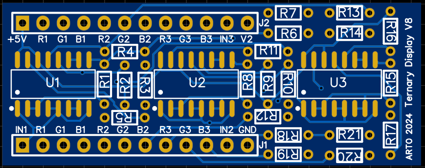
This board design concentrates on the 2 input Ternary Combinations.
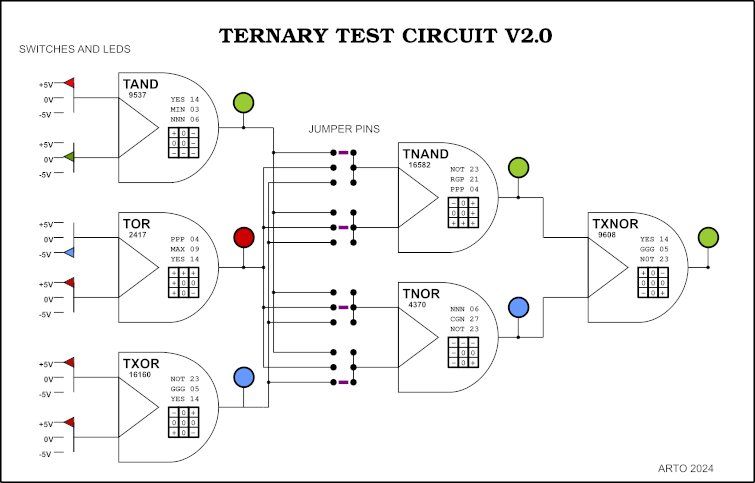
I had made many Ternary Gates, here are 2 preferred designs using optical relays, using a 28 pin form.
The display units are less demanding and can be designed in many ways, here are 3 designs, using 24 pins.
The V9 Ternary display unit requires 100 ohm resistors before grounding, if you use V7 or V8 you can just use shorting wires if you requires them, or just leave in the 100 ohm resistors. ( untested)
First of all the 6 switched inputs relates to three 2 input gates which are arranged to give you a maximum of choice.
The first 2 inputs A1 + B1 are directly combined in C1 to create the 2 output gate, designed by the links you combine in 12 pin matrix on the right side of each TNG2-1 chip.
To make your life easier I have put a number of gates that you can use on the bottom of the main board.
The LED outputs are in three groups:
1] switched inputs (6) A1 B1 A2 B2 A3 B3 2] output from each ternary gate (3) C1 C2 C3 3] output from combinations of 3 ternary gates D1 D2 4] output from the last 2 gates E1
To understand the Ternary Gate link matrix, here is a legend:
The jumper settings allows 81 variations, in 3 blocks -1 to 27, 28 to 54, 55 to 81;
I set the basic set up as number 67 from the list above. There are only 36 link combinations that include all three outputs from gates C (they form a top/bottom symmetrical list). Here are the sets:
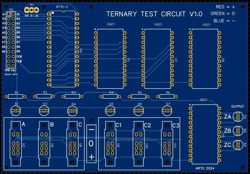
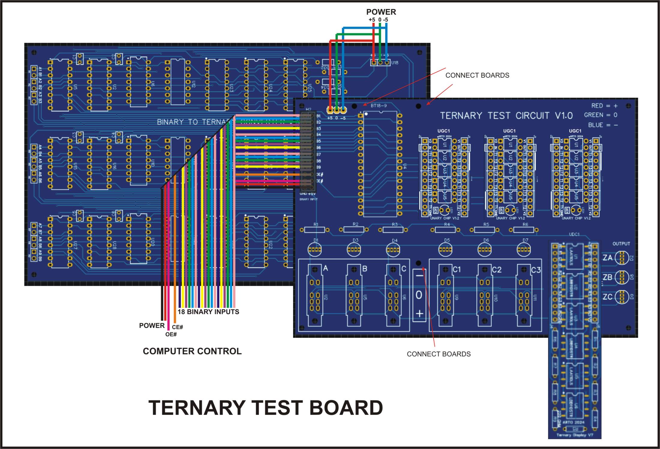
This board can accommodate 3 ternary chips the “BT18-9”, “UGC1” and “UDC1”, all of which are separate units, the BT18-9 needs either a set of ribbon cables with a socket or it can be directly connected with some HDR pins such as the connection diagram into the test board.
BT18-9
18 Binary paired Inputs (A1 B1) to (A9 B9) 9 Ternary outputs T0 to T8 OE# = output enable (you can set inputs then set to 0) CE# = chip enable (you must enable to 0 to start chip) +5V GND -5V
UGC1
1 Ternary input 1 Ternary output 1 led indictor of (-) 6 sets of programable inputs, in order
T1 T2 T3 T2 T3 T1 T3 T1 T2
T1 T3 T2 T2 T1 T3 T3 T3 T1
You can only connect 1 set at any one time, if you use a set of 3 jumper pins on all of the sets you could swap your combinations. These combinations will change your inputs into any one of six possibilities. This could also be done by using a analogue chip in a separate circuit.
UDC1
3 Ternary inputs 3 sets of 3 colour led outputs 3 sets of 3 colour led outputs (mirror of 1st set) So you could use these as Binary output switches or sensors as required. GND V1 = +5V V2 = spare 1 (-5v)
There are 3 ternary input switches (A B C) for all three RGB outputs (ZA ZB ZC) to function, there are also 3 selectors that need to be programmed first. Two of these are programmable by a binary source, while the other is by the onboard switches (C1 C2 C3). The current footprint of the display chip is 24pin pdip, even though the board is longer. As this is still only version 7, more work to do yet and I will eventually make it fit inside the boundary similar to the UGC1 board, on version 8 or 9. I am using optical relays in this design, something that I found useful in my ternary work.
Starting from a Binary input where you have 2 bits to make a ternary trit:
00 = + 10 = 0 01 = –
The bit combination “11” is not valid and will not be used even though it is available as a binary output. The ternary converter ignores it.
Here are the 27 Unary gate combinations that are available and the binary combinations that will create them all. The UGI is the “Unary Gate Index”, numbering of all the gates in a system I have shown on my previous blogs.
Starting with the A1 and B1 as the first pair, then the A2,B2 then A3,B3, these three sets will give you a Unary set of 3 that will configure the basic Unary Chip “UGC1” to one of the 27 gates.
The second set A4,B4 + A5,B5 + A6,B6 will configure the next UGC1 gate. The third set are the switches C1,C2,C3 these will give you another UGC1 gate for you to use.
The outputs ZA,ZB,ZC correspond to the input data A,B,C, where your programmed UGC1 gate is being used to compute your result into the Z Led outputs. Where:
Red = + Green = 0 Blue = –
The input switches A,B,C,C1,C2,C3 also have RGB LEDs.
I hope this might start your interest in Ternary Logic and Computation, regards Arto.
** I have added UDC1 V8 to the Zipfile **
Ternary Test Boards PCB1D Zipfile
Al the PCB and Schematics for this project.
EasyEDA files only.
As a hobbyist I am always trying to work out how certain technologies function, so I decided to look into the PAL, PLA and any programmable logic arrays. So instead of using them as most technicians do I decided to create my own, by standard logic gates and switches, as I am just as interested in the why as the how.
These are my versions of Programmable Logic Arrays based on 74LS chips and 2 position toggle switches. I could try and replicate a standard PAL or PLE chip, but that would just clutter my simple approach as a learning tool. I made them so you can jumper the IC socket into to an existing circuit to test your programming.
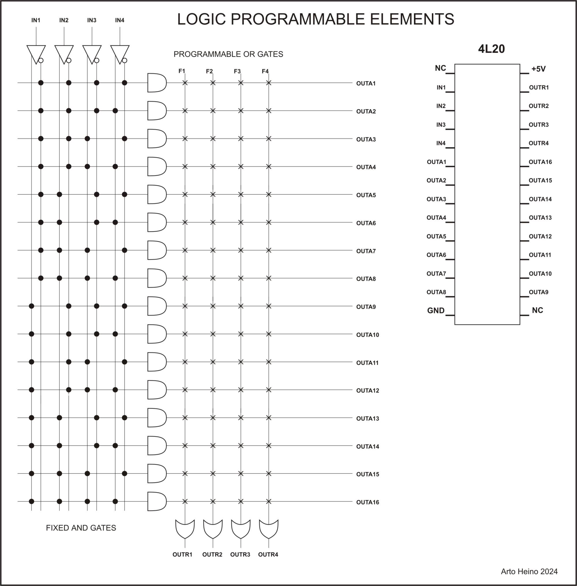
LPA-4H10
Using AND/OR arrays, the AND array is either on(throughput) or off(made high) and the OR array is a fixed set to give you the maximum of multiple of outputs (6). My design is based on four 8 input AND gates, which are selectable by 8 switches, giving you a maximum of 32 switches. Using the 4 input bits and it’s inversion to give you 8 internal inputs for each AND gate.
IN1 x IN1# x IN2 x IN2# x IN3 x IN3# x IN4 x IN4# = OUTA1
Your input IN1 to IN4 are you only inputs, all the logic combinations are after your initial input.
AND Gates
2 INPUT, where A=INv and B=INw and Z=OUTAy (v = 1 to 4, w = 1 to 4, y = 1 to 4 )
AND NOT NOT AND AND AFBT ATBF NOR A B Z A# B Z A B# Z A# B# Z --------- --------- --------- --------- 0 0 0 1 0 0 0 1 0 1 1 1 0 1 0 1 1 1 0 0 0 1 0 0 1 0 0 0 0 0 1 1 1 0 1 0 1 1 1 0 1 0 1 0 0 0 0 0
3 INPUT
A B C Z A# B C Z A B# C Z A B C# Z ------------------ 0 0 0 0 0 0 1 0 0 1 0 0 0 1 1 0 1 1 1 1 1 0 0 0 1 0 1 0 1 1 1 1 1 1 0 0 1 1 1 1 1 1 1 1
A B# C# Z A# B# C Z A# B C# Z A# B# C# Z ------------------ 0 1 1 0 1 1 1 1 0 1 0 0 1 1 1 1 0 0 1 0 1 1 1 1 0 0 0 0 1 1 1 1 1 1 0 0 1 0 1 0 1 0 0 0
The abbreviations AFBT and ATBF was devised by me to simplify some of the less known logic gates that are available to the binary combinations. All these odd types of gates can be created with AND, OR, XOR, NOR, XNOR or NAND gates with an inverter on one of the gates as well. I don’t know how useful my ideas are to those Engineers who were educated in Digital Logic, but as an intuitive tool that I have developed, it has given me an insight into applying digital Systems to my Ternary work. As Ternary logic has a massive (19683) number of 2 input elements, your mind boggles at the idea of “Truelean Logic” as opposed to “Boolean Logic” which has only 16 two input elements. Here is the Matrix I developed when I sorted my relay logic elements, it clearly shows how it was developed.
AFBT (AfBt)
Z = (A = False = 0) + (B = True = 1) = True = 1 Z only equals True when (A = False = 0) and (B = true = 1) all the rest are False = 0. If you look at the A input as inverted you will have the same as standard logic, as such:
My Symbol: ____ A ----\ \ | \---------- Z B ----/____|
De Morgans Symbol2 Gated Logic _____ _____ A ----O| \ A ---|>O--| \ | |------- Z = | |--- Z B -----|_____/ B --------|_____/
ATBF (AtBf)
Z = (A = True = 1) + (B = False = 0) = True = 1 Z only equals True when (A = True = 1) and (B = False = 0) all the rest are False = 0. If you look at the B input as inverted you will have the same as standard logic, as such:
My Symbol: _____ A ----\ | | /---------- Z B ----/___/
De Morgans Symbol2 Gated Logic _____ _____ A -----| \ A --------| \ | |------- Z = | |------ Z B ----O|_____/ B ---|>O--|_____/
My Symbolism for multiple inputs
AfBCDEFGt

           *     *     *     *     *     *
Z = (A=0)+(B=1)+(C=1)+(D=1)+(E=1)+(F=1)+(G=1)=1

ACDEFGtBf

     *           *     *     *     *     *
Z = (A=1)+(B=0)+(C=1)+(D=1)+(E=1)+(F=1)+(G=1)=1

ABDFGtCEf

     *     *           *           *     *
Z = (A=1)+(B=1)+(C=0)+(D=1)+(E=0)+(F=1)+(G=1)=1
LPA Logic
The output from the AND array goes into a OR array that is set by 2 inputs using a OR combination, such as:
As you can see there are no more possible combinations than these six for a 2 input OR gate. Another added output is the ANDed output before the ORing which gives you another 4 outputs to use, giving you a total of 10 outputs.
Example 1a:
Here are the equations you can use, by using only IN1 and IN2 as your inputs:
So if you use two inputs, also using only 2 switchs F1 ans F2 of both inputs. Thus you get:
“#” = inversion
“^” = high = 1 (off)
OUTR1 = ((IN1 x F1) x (IN1# x F2^)) + ((IN2 x F1^) x (IN2# x F2))
When a switch “F” is on, then it equals the “IN” input. If “F” if off the it is high (=1).
If, IN1 = 1/0 and F1 is on and F2 is off (1), the rest of the switches are off (1) IN1(F3-F8). Every even switch uses the inverted version of the odd input going to the internal OR inputs.
also, IN2 = 1/0 and F1 is off (1) and F1 is on, the rest of the switches will be off (1) IN2(F3-F8)
IN1(F2) IN2(F1) = switch to high
             AND				OR
             _____
IN1 -0101---|  F1 \  	0101	             ______
            |      |------- OUTA1 ---0101 ---\      \
IN1 -0101--O|__F2_/ 	1111	              |      \
                                              |       \__OUTR1_1101
             _____		              |       /
IN2 -0110---|  F1 \  	1111	              |      /
            |      |------- OUTA2 ---1001 ---/______/
IN2 -0110--O|__F2_/ 	1001
This will give you output to the OUTR1 line, the OUTA1 and OUTA2. This is the output when you swutch IN1(F2) and IN2(F1) to high;
If IN1 = 0 and IN2 = 0 then OUTR1 = 1 , OUTA1 = 0 , OUTA2 = 1 If IN1 = 1 and IN2 = 0 then OUTR1 = 1 , OUTA1 = 1 , OUTA2 = 1 If IN1 = 0 and IN2 = 1 then OUTR1 = 0 , OUTA1 = 0 , OUTA2 = 0 If IN1 = 1 and IN2 = 1 then OUTR1 = 1 , OUTA1 = 1 , OUTA2 = 0
Where switch position “on” allows your input to go through the circuit, while “off” is only “high” (1) so the AND gate now is one less than your total maximum of 8. So if you switch all 8 to “off” this input will be only be a “1”, giving you a “1” on the input to one of the set OR matrix inputs.
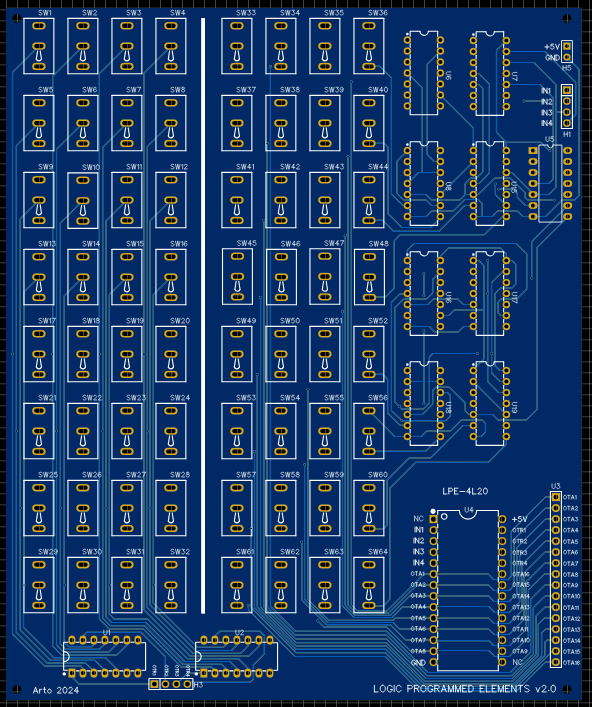
LPE-4L20
You get 4 inputs plus its internal inversions giving you 4 outputs (ORed) and 16 AND combinations. The off switch position is low, thus negating it throughput.
X = input o = inverted input
My first AND Matrix;
1 2 3 4 5 6 7 8 9 1 1 1 1 1 1 1
                  0 1 2 3 4 5 6
x x x x . x x . x . . x . . . .
. . . . o . . o . o o . o o o o

x x x . x x . . . x x . x . . .
. . . o . . o o o . . o . o o o

x x . x x . . x x . x . . x . .
. . o . . o o . . o . o o . o o

x . x x x . x x . x . . . . x .
. o . . . o . . o . o o o o . o
I was going to use this internal format, until I decided to use the standard PLE arrangement.
--------------------------------
   |   |   |   |   |   |   |
1 2 3 4 5 6 7 8 9 1 1 1 1 1 1 1		Net     AND Inverter output
                  0 1 2 3 4 5 6
. . . . . . . . x x x x x x x x   	H1  	A   1A
o o o o o o o o . . . . . . . .		U5_2	    1Y

. . . . x x x x . . . . x x x x 	H2	B   2A
o o o o . . . . o o o o . . . .		U5_4	    2Y

. . x x . . x x . . x x . . x x 	H3	C   3A
o o . . o o . . o o . . o o . .		U5_6	    3Y

. x . x . x . x . x . x . x . x		H4	D   4A
o . o . o . o . o . o . o . o .		U5_8	    4Y
So if you want to implement a 4 input XOR gate:
FnXOR = XOR (IN1 IN1# IN2 IN2# IN3 IN3# IN4 IN4#)
 =
(IN1 X IN2# X IN3# X IN4#) +
(IN1# X IN2 X IN3# X IN4#) +
(IN1# X IN2# X IN3 X IN4#) +
(IN1# X IN2# X IN3# X IN4) +
(IN1 X IN2 X IN3 X IN4#) +
(IN1 X IN2 X IN3# X IN4) +
(IN1 X IN2# X IN3 X IN4) +
(IN1# X IN2 X IN3 X IN4)
Switches used: (from 1 to 64) 5 9 17 29 33 45 53 57 – or – first column (1 to 16) 2 3 5 8 9 12 14 15 are ON all other switches are OFF
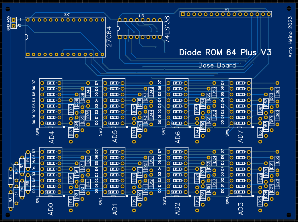
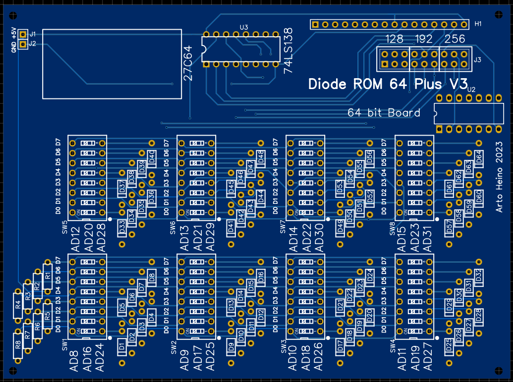
As my research moves along, I decided to create a Diode Memory unit first for binary use, before I implement the ternary memory version. I designed 2 types of boards, the first is the base board which is the first 64 bits or 8 bytes, the 2nd board can be stacked on top to create 128 bits or 16 bytes with more boards on top for 192/256 bits or 24/32 bytes. I will be building these soon, as these designs have not been tested yet, I suggest checking my work, I will confirm these in another blog.
The ROM choice was a 27C64 which is a 8Kx8 and is very popular, available in general stock and I will use it in further designs, the decoder is a 74LS138 which seems to be a great choice for this simple project. The only problem I had was the 138 has only 3 bits to decode, so I had to add a few extra bit of routing to create 32 bytes. The 138 has 3 enable lines GA_, GB_, G1, so the first block I put G1 high and GA_and GB_ would be enabled when both are low, these are from the A3 and A4 lines which are low. The second block I put GA_ low to ground with GB_ and G1 would be A4 as low and A3 as high. As you can see by the diagram I swapped A3 and A4 with GA grounded for the 3rd block, the last block I used an inverter on GB_ from A3 which must be high,
If you are not using 32 bytes then you can ignore the 74LS04 connection. To use each block you must bridge the labelled connectors with jumpers. The Parts list for 2 boards are:
SK1 = 28 pin DIP socket with extended legs
H1 = 16 Pin socket with extended legs x 2
U3 = 74LS138 x 2
R1-R8 = 10K resistors x 2
D1-D64 = 1N4148 Diodes x 2
SW1-SW8 = 8 sw DIP x 2
J1-J2 = Pin for Power x 2
Each corner has 2mm holes , add crews and extended legs as needed x 2
If you choose to build it, you will be limited to 32 bytes. To test the unit you could plug it into to a EPROM reader. My next version should allow up to 256 bytes or more. Regards Arto.
Diode ROM PCB1C Zipfile
All the PCB and Schematics for this project. EasyEDA files only.
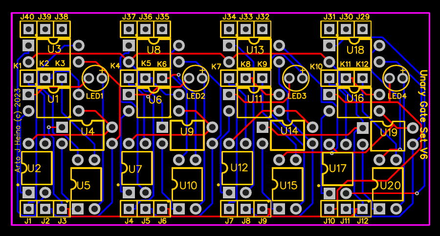
To start the journey of discovery, we must have all the building blocks and tools ready to use as creativity requires a selective group of useful mechanisms to achieve a modicum of feed back to keep the momentum going forward towards interesting and useful discoveries. The Ternary building block are here, along with a Binary controller that you can use to design your Logic elements as needed. I have shown previous Unary gates and they are still usable in these designs. I decided to put 4 gates in one unit so wiring can be simplified when you create the 2/3/4 input gates. For a 2 input gate you need 3 gates for the columns and a summing gate and 3 gates for the rows a summing gate for the rows and the result. This makes it simpler, you will only need 2 unary boards for an 2 input gate, a base board was designed to make this easier, these can be stacked, as high as required.
Parts List for each Unary Gate V6
U1,U3,U4 _________G3VM-353A U2,U5 ____________G3VM-61A1 U6,U8,U9 _________G3VM-353A U7,U10 ___________G3VM-61A1 U11,U13,U14 ______G3VM-353A U8,U15 ___________G3VM-61A1 U16,U18,U19 ______G3VM-353A U17,U20 __________G3VM-61A1 LED1,2,3,4 ________3mm Blue 36 x ______________Male/Female headers 20 x ______________4 Pin sockets (if required) 1 x _______________Unary Board V6
Parts List for Base Boards
4 x _______________24Pin Fmale Header 8 x _______________3 Pin
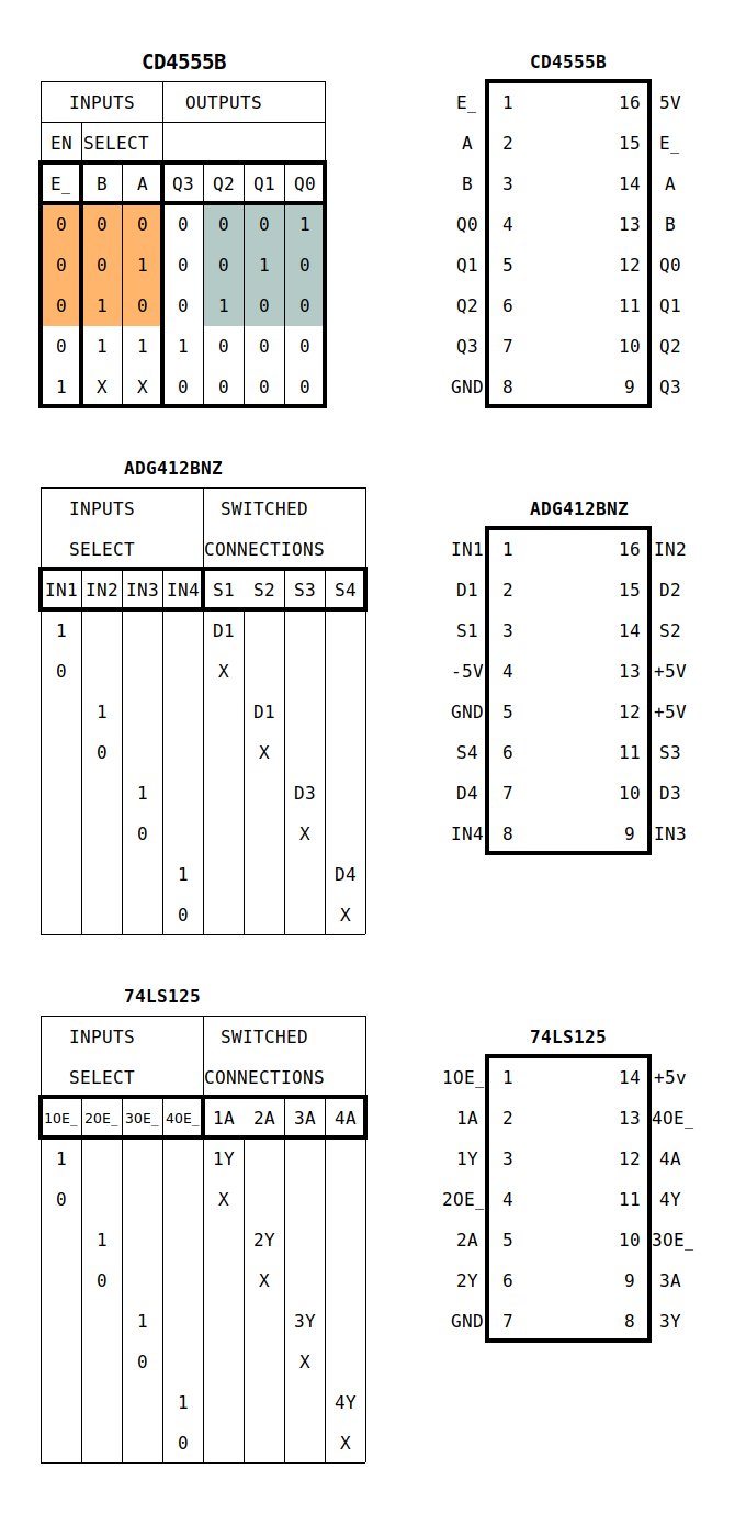
Parts List for Binary to Ternary Gate Selector Board
6 x _______________CD4555BE 9 x _______________ADG412BNZ C1,C2,C3,C4,C5,C6 _100 nF Caps D1-D12 ___________1N4007 D19,D20,D21,D22 __1N4007 1 x _______________LM7805 1 x _______________LM7905 C7,C10,C12,C22 ___47uF Electrolytic Caps Led1 _____________Led R1 _______________1K 3 x _______________6 Pin 3 x _______________5 Pin 15 x ______________8 Pin Dip 1 x _______________7 Pin Dip 1 x _______________74LS125
1 x _______________LAA110LS 1 x _______________LBB110STR 3 x _______________220 Ohm 3 x _______________1xPin hdrs 2.54 1 x _______________4 pin hdr 1.27 1 x _______________RGB PCB board
Parts List for TMS9995 Board
1 x ________U8 ____74LS138 1 x ________U5 ____74LS32 1 x ________U6 ____MAX232CPE 1 x ________U7 ____TMS9902 1 x _____U11+U12__TMS9901 x2 1 x ________U1 ____TMS9995 1 x ________U4 ____74LS04 1 x ________U3 ____62256-07 SRAM 1 x ________U2 ____M27C256 EPROM + Binary Data Cortex + Terminal 1 x _______________DB9 RS232 RA port 1 x _______________Header 6 Pin C1-C8 ____________100nF C11,C12___________100nF C16 -C20 __________1uF Electrolyticn R1________________10K R2 – R6____________1K C13, C14 __________15pF X1 _______________12 Mhz XTAL 1 x _______________LED21 LED indicator 1 x _______________SW4 Micro switch C15 ______________10nF 4 x _______________10 pin RA Male Pin Headers 1 x ________U9 ____LM7805 C22, C23 __________47Uf DC1 ______________9v input Jack 3 x________________40 Pin Dip 2 x _______________ 28 Pin Dip 2 x _______________ 14 Pin Dip 2 x _______________ 16 Pin Dip 1 x _______________ 18 Pin Dip 1 x _______________TMS9995 SBC PCB Board (Conner Stuarts Design)
Boards
Unary Gate Base Board V6 Unary Gate Base Board Singles V6 Binary to Ternary Gate Controller V1 Ternary Input Switches Ternary Bit Display TMS9995 SBC
Each Unary board consists of 4 separate Unary Gates they can be used as a set or individually, depending which base board you use.
The Unary Gate Base Board has been configured as a 2 input gate A, B and the result in C.
The Unary Gate Base Board Singles is configured to use as either a 2 input gate by wiring it as required or as single chains or groups.
J1, J4, J7, J10 are your ternary inputs, while J2, J5, J8, J11 are your outputs to each gate.
K1, K2, K3 are configurable with J40, J39, J38 as a matrix to give you all 27 Unary configurations. The interconnections are configurable with a small 6 pin cross connected board, or you can use jumper cables if you choose.
Controller Board
This has a 12vac input and 18+3 pin binary input and a 3 pin ternary output. It was designed to connect to a TMS9995 SBC with CRU outputs and have software to control the gate configuration in hardware.
With Five Boards there are 45 binary controls which will give you a Ternary Multiplexer made of five 2 input gates and 3 Unary gates. Once you have tested and configured your logic, then you can use the base board with plugin matrix connectors as your final gate design.
Setting Your Bits
H1, H2 and H3 are your binary control bits to select each gate type. You select 6 bits to as either decimal or Hex to each unary port. I added U28(74LS125) and U29 3 pin header which is used to switch each gate on, under software control as required.
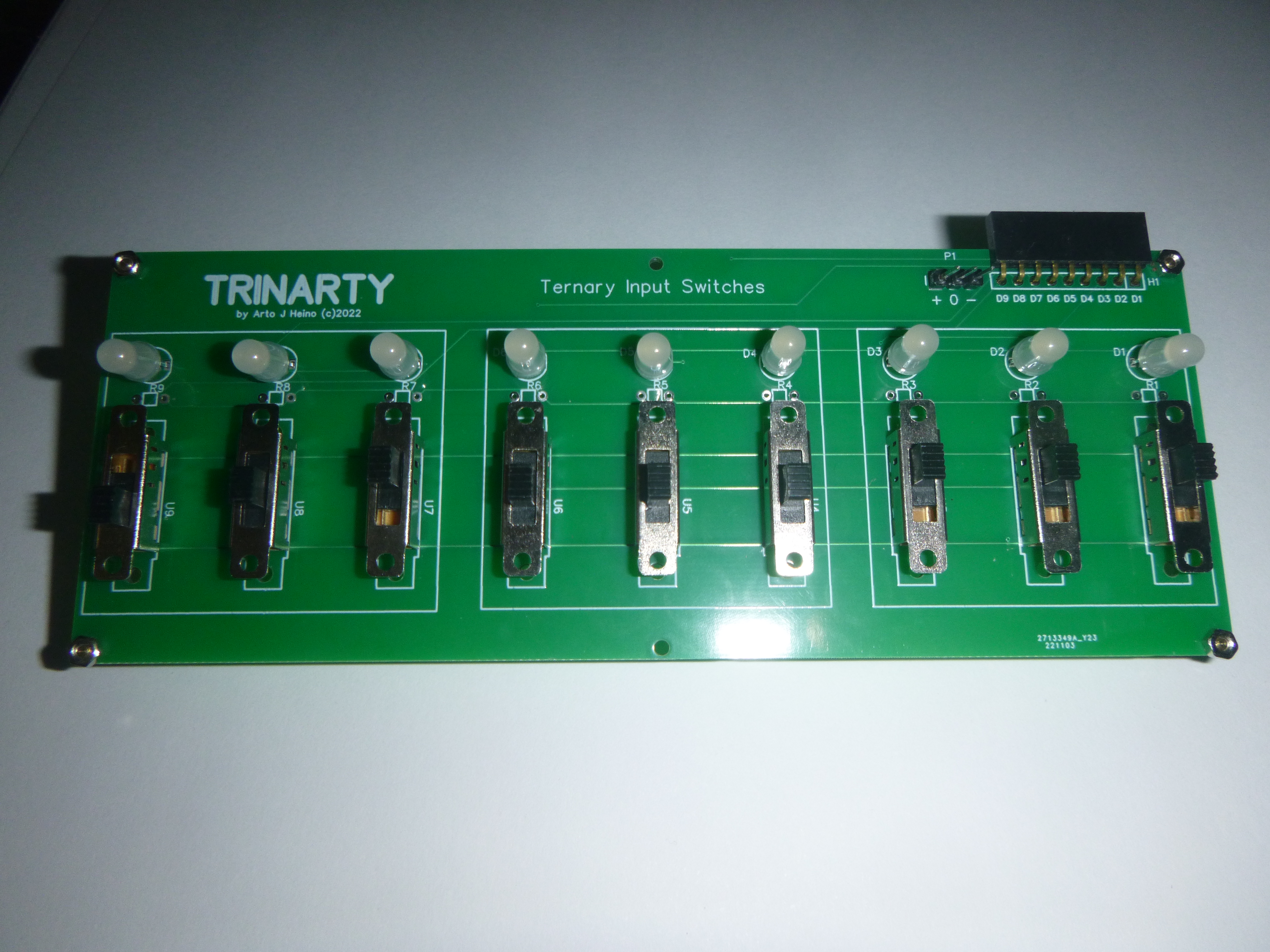
Ternary Input Switches
This board has 9 ternary outputs and can be used to control the A+B inputs on the Unary boards. There is 9 RGB indicators for the slide switches, Red = +5v , Green = 0v , Blue = -5v.
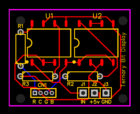
Ternary Bit Display
This small board gives you a visual indication of your output bits, Red = +5v , Green = 0v , Blue = -5v
Listed below is the Program to control the Ternary Gate Selector. If you want to attach more Selector boards you will need to expand the CRU outputs. I have left the header J5 to allow CE for more TMS9901 to be added at some point. The next version will also have have mounting board for 4 more chips, giving a total of 96 outputs.
Where 21 are needed for each 2 input gate, this allows control of 4 2 input gates, 84 pins , leaving you 12 spare pins for other controls.
This is a Cortex Basic program to control one two input gate.
8 REM TERNARY GATE CONTROL 9 REM *** BY ARTO HEINO 2023 ** 10 REM OUTPUT ON 9901 PORT BIT 0 to bit 20 (21 BITS) 11 REM TO CONTROL TERNARY 18 BIT GATES + 3 BIT CONTROL 12 REM 13 REM SETUP BASE ADDRESS OF 9901 to 64 decimal = >0040 HEX 14 BASE 64 15 DIM TR(27,6) 17 REM DISABLE EACH CD4555BE CHIP 18 CRB(16+18)=0 19 CRB(16+19)=0 20 CRB(16+20)=0 24 REM LOAD 27 TERNARY GATE BIT DATA 25 RESTORE 27 FOR Z=1 TO 27 28 FOR X = 1 TO 6 29 READ TR(Z,X) 30 NEXT X 31 NEXT Z 32 REM SELECT 3 GATES 33 FOR A=1 TO 3 36 PRINT “COLUMN “; A 38 PRINT “SELECT GATE 1 TO 27” 39 INPUT GT 40 IF GT<1 OR GT>27 THEN GOTO 38 42 FOR BT=1 T0 6 45 REM SET HIGH OR LOW 48 CRB(15+BT+(A*6-6)) =TR(GT,BT) 56 NEXT BT 57 NEXT A 60 REM ENABLE EACH CD4555BE CHIP 61 CRB(16+18)=1 62 CRB(16+19)=1 63 CRB(16+20)=1 64 END 65 REM DATA FOR GATES 66 REM H1 + H2 + H3 101 DATA 0,0,0,0,0,0 102 DATA 1,0,0,0,0,0 103 DATA 0,1,0,0,0,0 104 DATA 0,0,1,0,0,0 105 DATA 1,0,1,0,0,0 106 DATA 0,1,1,0,0,0 107 DATA 0,0,0,1,0,0 108 DATA 1,0,0,1,0,0 109 DATA 0,1,0,1,0,0 110 DATA 0,0,0,0,1,0 111 DATA 1,0,0,0,1,0 112 DATA 0,1,0,0,1,0 113 DATA 0,0,1,0,1,0 114 DATA 1,0,1,0,1,0 115 DATA 0,1,1,0,1,0 116 DATA 0,0,0,1,1,0 117 DATA 1,0,0,1,1,0 118 DATA 0,1,0,1,1,0 119 DATA 0,0,0,0,0,1 120 DATA 1,0,0,0,0,1 121 DATA 0,1,0,0,0,1 122 DATA 0,0,1,0,0,1 123 DATA 1,0,1,0,0,1 124 DATA 0,1,1,0,0,1 125 DATA 0,0,0,1,0,1 126 DATA 1,0,0,1,0,1 127 DATA 0,1,0,1,0,1
Here is the layout for the SBC and the Ternary Gates.
An alternative design without the SBC and just putting units together.
Here are a few pictures regarding some of the components.
This is the CODE for the 27 selections of Unary gates, H1,H2,H3 CRU outputs.
Here are the PCB’s for the Basic boards.
If you want to see more of this type of content, I would appreciate your support to help pay for more original designs and parts. I hope you enjoy this work, regards Arto.
Ternary PCB1A Zipfile
All the PCB and Schematics for this project. EasyEDA files only.
An error has occurred; the feed is probably down. Try again later.
Join 130 other subscribers
Published material Link
Talking to the Birds
Book Available NOW
At Amazon
At Createspace
https://www.createspace.com/4513692
______________________
Cartoons
http://www.scribd.com/doc/106684504/Scraps-Sketches-and-Satire
_______________________
Magic Square
http://www.scribd.com/doc/33050524/The-Magic-Square-of-Three-Crystal