Ternary Test Circuits
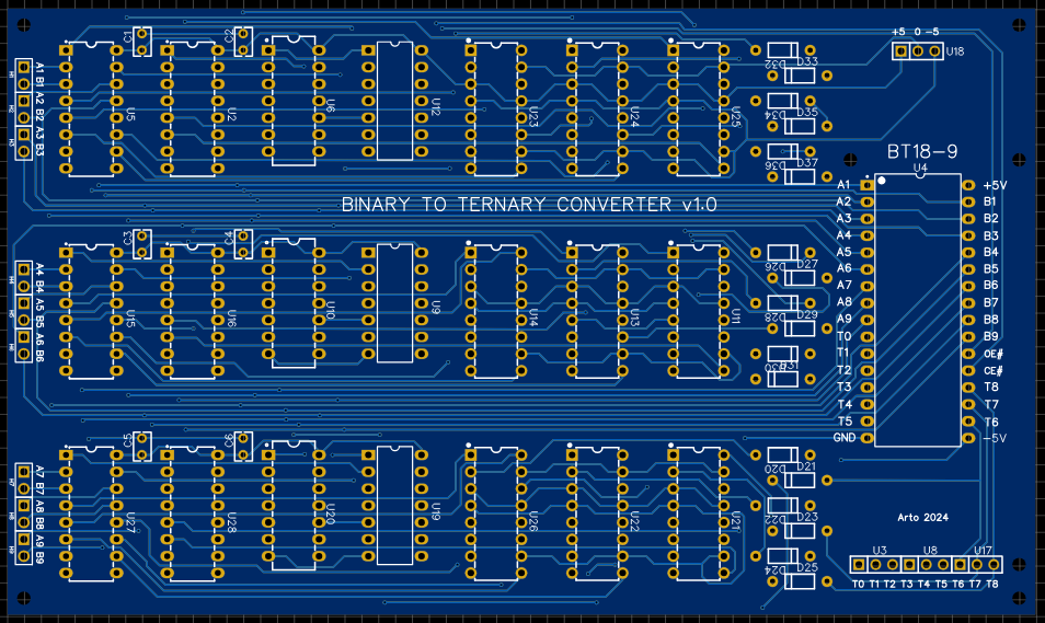
This board can accommodate 3 ternary chips the “BT18-9”, “UGC1” and “UDC1”, all of which are separate units, the BT18-9 needs either a set of ribbon cables with a socket or it can be directly connected with some HDR pins such as the connection diagram into the test board.
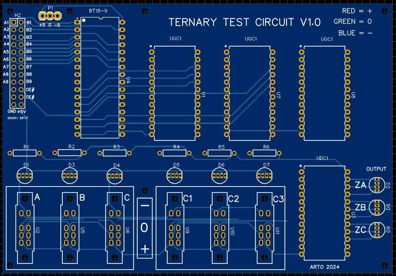
BT18-9
18 Binary paired Inputs (A1 B1) to (A9 B9)
9 Ternary outputs T0 to T8
OE# = output enable (you can set inputs then set to 0)
CE# = chip enable (you must enable to 0 to start chip)
+5V
GND
-5V
UGC1
1 Ternary input
1 Ternary output
1 led indictor of (-)
6 sets of programable inputs, in order
T1 T2 T3
T2 T3 T1
T3 T1 T2
T1 T3 T2
T2 T1 T3
T3 T3 T1
You can only connect 1 set at any one time, if you use a set of 3 jumper pins on all of the sets you could swap your combinations. These combinations will change your inputs into any one of six possibilities. This could also be done by using a analogue chip in a separate circuit.

UDC1
3 Ternary inputs
3 sets of 3 colour led outputs
3 sets of 3 colour led outputs (mirror of 1st set) So you could use these as Binary output switches or sensors as required.
GND
V1 = +5V
V2 = spare 1 (-5v)

There are 3 ternary input switches (A B C) for all three RGB outputs (ZA ZB ZC) to function, there are also 3 selectors that need to be programmed first. Two of these are programmable by a binary source, while the other is by the onboard switches (C1 C2 C3). The current footprint of the display chip is 24pin pdip, even though the board is longer. As this is still only version 7, more work to do yet and I will eventually make it fit inside the boundary similar to the UGC1 board, on version 8 or 9. I am using optical relays in this design, something that I found useful in my ternary work.
Starting from a Binary input where you have 2 bits to make a ternary trit:
00 = +
10 = 0
01 = –
The bit combination “11” is not valid and will not be used even though it is available as a binary output. The ternary converter ignores it.
Here are the 27 Unary gate combinations that are available and the binary combinations that will create them all. The UGI is the “Unary Gate Index”, numbering of all the gates in a system I have shown on my previous blogs.

Starting with the A1 and B1 as the first pair, then the A2,B2 then A3,B3, these three sets will give you a Unary set of 3 that will configure the basic Unary Chip “UGC1” to one of the 27 gates.
The second set A4,B4 + A5,B5 + A6,B6 will configure the next UGC1 gate. The third set are the switches C1,C2,C3 these will give you another UGC1 gate for you to use.
The outputs ZA,ZB,ZC correspond to the input data A,B,C, where your programmed UGC1 gate is being used to compute your result into the Z Led outputs. Where:
Red = +
Green = 0
Blue = –
The input switches A,B,C,C1,C2,C3 also have RGB LEDs.
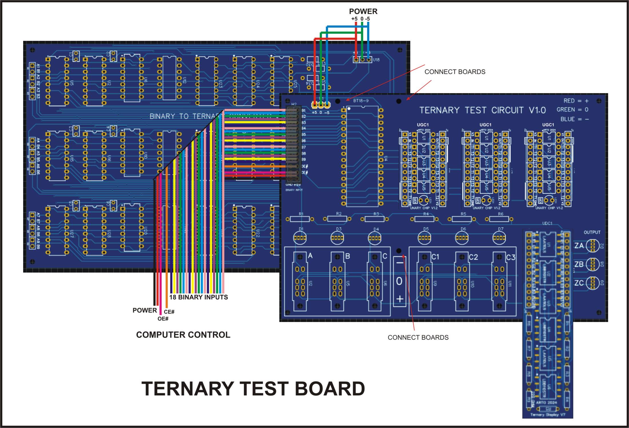
I hope this might start your interest in Ternary Logic and Computation, regards Arto.
** I have added UDC1 V8 to the Zipfile **

Ternary Test Boards PCB1D Zipfile
Al the PCB and Schematics for this project. EasyEDA files only.
$15.00
