Switchable Logic Arrays
As a hobbyist I am always trying to work out how certain technologies function, so I decided to look into the PAL, PLA and any programmable logic arrays. So instead of using them as most technicians do I decided to create my own, by standard logic gates and switches, as I am just as interested in the why as the how.
These are my versions of Programmable Logic Arrays based on 74LS chips and 2 position toggle switches. I could try and replicate a standard PAL or PLE chip, but that would just clutter my simple approach as a learning tool. I made them so you can jumper the IC socket into to an existing circuit to test your programming.
LPA-4H10
Using AND/OR arrays, the AND array is either on(throughput) or off(made high) and the OR array is a fixed set to give you the maximum of multiple of outputs (6). My design is based on four 8 input AND gates, which are selectable by 8 switches, giving you a maximum of 32 switches. Using the 4 input bits and it’s inversion to give you 8 internal inputs for each AND gate.
IN1 x IN1# x IN2 x IN2# x IN3 x IN3# x IN4 x IN4# = OUTA1
Your input IN1 to IN4 are you only inputs, all the logic combinations are after your initial input.

AND Gates
2 INPUT, where A=INv and B=INw and Z=OUTAy (v = 1 to 4, w = 1 to 4, y = 1 to 4 )
			AND			NOT
			NOT			AND
AND			AFBT			ATBF			NOR
A	B	Z	A#	B	Z	A	B#	Z	A#	B#	Z
---------		---------		---------		---------
0	0	0	1	0	0	0	1	0	1	1	1
0	1	0	1	1	1	0	0	0	1	0	0
1	0	0	0	0	0	1	1	1	0	1	0
1	1	1	0	1	0	1	0	0	0	0	0

3 INPUT

A	B	C	Z	A# B  C  Z	A  B# C  Z	A  B  C#  Z
------------------
0       0       0       0
0	0	1	0
0	1	0	0
0	1	1	0	1  1  1  1
1	0	0	0
1	0	1	0			1  1  1  1
1	1	0	0					1  1  1  1
1	1	1	1


A	B#	C#	Z	A# B# C  Z	A# B  C# Z	A# B# C# Z
------------------
0       1       1       0					1  1  1  1
0	1	0	0	1  1  1  1
0	0	1	0			1  1  1  1
0	0	0	0
1	1	1	1
1	1	0	0
1	0	1	0
1	0	0	0

4 INPUT

                                                                        ZA# ZA# ZA# ZB#
					ZA# ZA# ZA# ZB# ZB# ZC#		ZB# ZB# ZC# ZC#
A B C D Z	ZA# ZB# ZC# ZD#		ZB# ZC# ZD# ZC# ZD# ZD#		ZC# ZD# ZD# ZD#
---------
0 0 0 0	0
0 0 0 1 0								1
0 0 1 0 0								    1
0 0 1 1 0				1				        1
0 1 0 0 0				    1
0 1 0 1 0				        1
0 1 1 0 0
0 1 1 1 0	1
1 0 0 0 0	              		                     		            1
1 0 0 1 0				            1
1 0 1 0 0				                1
1 0 1 1 0	    1
1 1 0 0 0				                    1
1 1 0 1 0	        1
1 1 1 0 0	            1
1 1 1 1 1
My Own Symbolism
The abbreviations AFBT and ATBF was devised by me to simplify some of the less known logic gates that are available to the binary combinations. All these odd types of gates can be created with AND, OR, XOR, NOR, XNOR or NAND gates with an inverter on one of the gates as well. I don’t know how useful my ideas are to those Engineers who were educated in Digital Logic, but as an intuitive tool that I have developed, it has given me an insight into applying digital Systems to my Ternary work. As Ternary logic has a massive (19683) number of 2 input elements, your mind boggles at the idea of “Truelean Logic” as opposed to “Boolean Logic” which has only 16 two input elements. Here is the Matrix I developed when I sorted my relay logic elements, it clearly shows how it was developed.

AFBT (AfBt)
Z = (A = False = 0) + (B = True = 1) = True = 1
Z only equals True when (A = False = 0) and (B = true = 1) all the rest are False = 0. If you look at the A input as inverted you will have the same as standard logic, as such:
My Symbol:
      ____
A ----\   \
       |   \---------- Z
B ----/____|

De Morgans Symbol		2 Gated Logic
        _____	                           _____
A ----O|     \  		A ---|>O--|     \
       |      |------- Z  =		  |      |--- Z
B -----|_____/ 			B --------|_____/
ATBF (AtBf)
Z = (A = True = 1) + (B = False = 0) = True = 1
Z only equals True when (A = True = 1) and (B = False = 0) all the rest are False = 0. If you look at the B input as inverted you will have the same as standard logic, as such:
My Symbol:
      _____
A ----\    |
       |   /---------- Z
B ----/___/

De Morgans Symbol		2 Gated Logic
        _____				   _____
A -----|     \  		A --------|     \
       |      |------- Z  =		  |      |------ Z
B ----O|_____/ 			B ---|>O--|_____/
My Symbolism for multiple inputs
AfBCDEFGt

           *     *     *     *     *     *
Z = (A=0)+(B=1)+(C=1)+(D=1)+(E=1)+(F=1)+(G=1)=1

ACDEFGtBf

     *           *     *     *     *     *
Z = (A=1)+(B=0)+(C=1)+(D=1)+(E=1)+(F=1)+(G=1)=1

ABDFGtCEf

     *     *           *           *     *
Z = (A=1)+(B=1)+(C=0)+(D=1)+(E=0)+(F=1)+(G=1)=1
LPA Logic
The output from the AND array goes into a OR array that is set by 2 inputs using a OR combination, such as:
OUTA1 OUTA2 = OUTR1
OUTA2 OUTA3 = OUTR2
OUTA3 OUTA4 = OUTR3
OUTA1 OUTA3 = OUTR4
OUTA2 OUTA4 = OUTR5
OUTA1 OUTA4 = OUTR6
As you can see there are no more possible combinations than these six for a 2 input OR gate. Another added output is the ANDed output before the ORing which gives you another 4 outputs to use, giving you a total of 10 outputs.
Example 1a:
Here are the equations you can use, by using only IN1 and IN2 as your inputs:
So if you use two inputs, also using only 2 switchs F1 ans F2 of both inputs.
Thus you get:
“#” = inversion
“^” = high = 1 (off)
OUTR1 = ((IN1 x F1) x (IN1# x F2^)) + ((IN2 x F1^) x (IN2# x F2))
When a switch “F” is on, then it equals the “IN” input. If “F” if off the it is high (=1).
If, IN1 = 1/0 and F1 is on and F2 is off (1), the rest of the switches are off (1) IN1(F3-F8). Every even switch uses the inverted version of the odd input going to the internal OR inputs.
also, IN2 = 1/0 and F1 is off (1) and F1 is on, the rest of the switches will be off (1) IN2(F3-F8)
IN1(F2) IN2(F1) = switch to high
             AND				OR
             _____
IN1 -0101---|  F1 \  	0101	             ______
            |      |------- OUTA1 ---0101 ---\      \
IN1 -0101--O|__F2_/ 	1111	              |      \
                                              |       \__OUTR1_1101
             _____		              |       /
IN2 -0110---|  F1 \  	1111	              |      /
            |      |------- OUTA2 ---1001 ---/______/
IN2 -0110--O|__F2_/ 	1001
This will give you output to the OUTR1 line, the OUTA1 and OUTA2.
This is the output when you swutch IN1(F2) and IN2(F1) to high;
If IN1 = 0 and IN2 = 0 then OUTR1 = 1 , OUTA1 = 0 , OUTA2 = 1
If IN1 = 1 and IN2 = 0 then OUTR1 = 1 , OUTA1 = 1 , OUTA2 = 1
If IN1 = 0 and IN2 = 1 then OUTR1 = 0 , OUTA1 = 0 , OUTA2 = 0
If IN1 = 1 and IN2 = 1 then OUTR1 = 1 , OUTA1 = 1 , OUTA2 = 0
Where switch position “on” allows your input to go through the circuit, while “off” is only “high” (1) so the AND gate now is one less than your total maximum of 8. So if you switch all 8 to “off” this input will be only be a “1”, giving you a “1” on the input to one of the set OR matrix inputs.

LPE-4L20
You get 4 inputs plus its internal inversions giving you 4 outputs (ORed) and 16
AND combinations. The off switch position is low, thus negating it throughput.
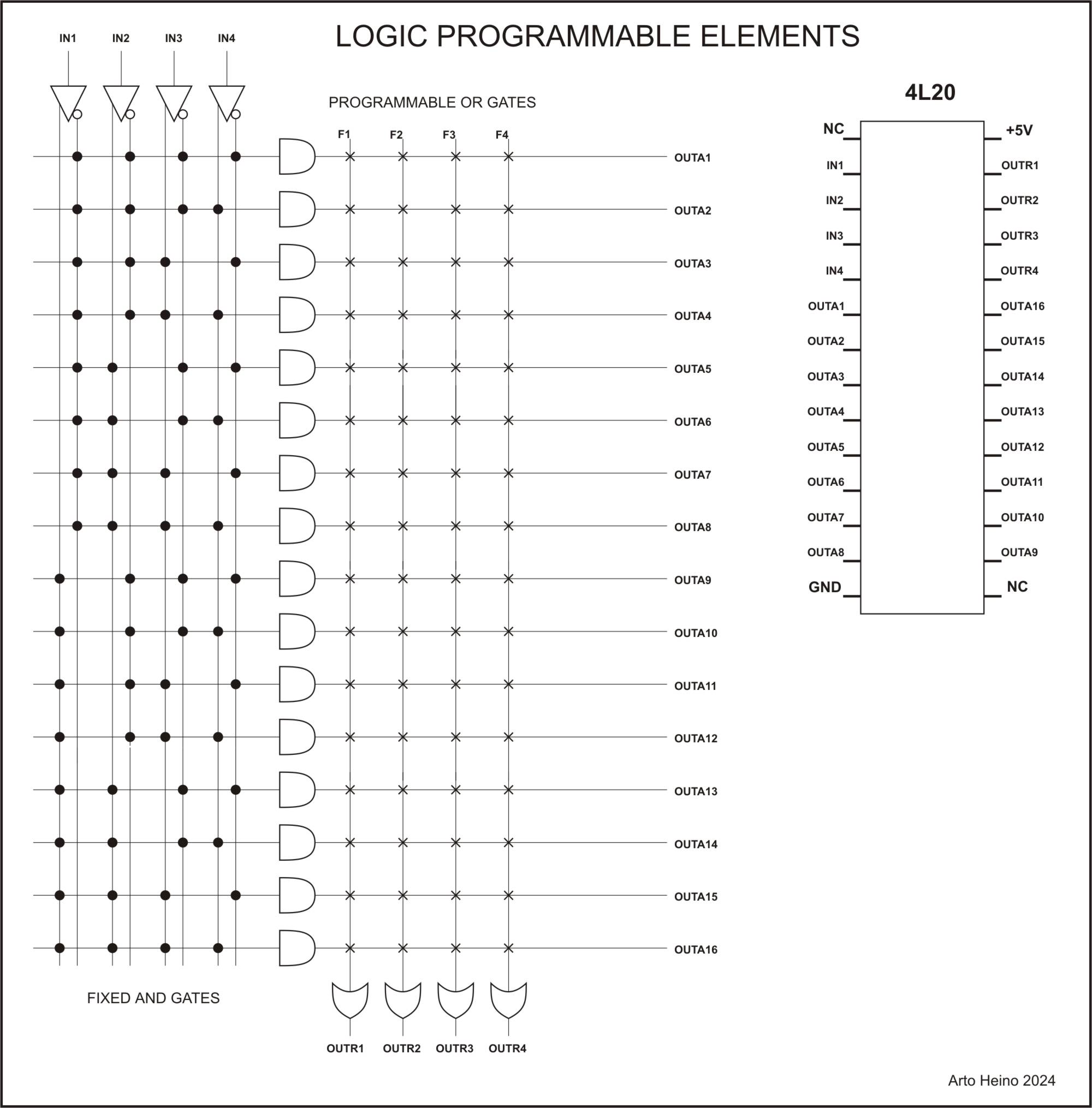
X = input
o = inverted input
My first AND Matrix;
1 2 3 4 5 6 7 8 9 1 1 1 1 1 1 1
                  0 1 2 3 4 5 6
x x x x . x x . x . . x . . . .
. . . . o . . o . o o . o o o o

x x x . x x . . . x x . x . . .
. . . o . . o o o . . o . o o o

x x . x x . . x x . x . . x . .
. . o . . o o . . o . o o . o o

x . x x x . x x . x . . . . x .
. o . . . o . . o . o o o o . o
I was going to use this internal format, until I decided to use the standard PLE arrangement.
--------------------------------
   |   |   |   |   |   |   |
1 2 3 4 5 6 7 8 9 1 1 1 1 1 1 1		Net     AND Inverter output
                  0 1 2 3 4 5 6
. . . . . . . . x x x x x x x x   	H1  	A   1A
o o o o o o o o . . . . . . . .		U5_2	    1Y

. . . . x x x x . . . . x x x x 	H2	B   2A
o o o o . . . . o o o o . . . .		U5_4	    2Y

. . x x . . x x . . x x . . x x 	H3	C   3A
o o . . o o . . o o . . o o . .		U5_6	    3Y

. x . x . x . x . x . x . x . x		H4	D   4A
o . o . o . o . o . o . o . o .		U5_8	    4Y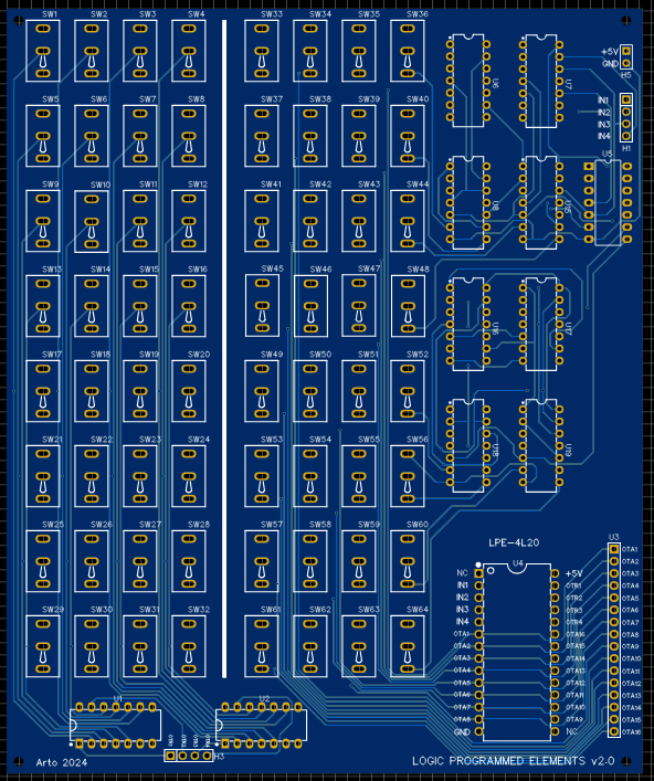
So if you want to implement a 4 input XOR gate:
FnXOR = XOR (IN1 IN1# IN2 IN2# IN3 IN3# IN4 IN4#)
 =
(IN1 X IN2# X IN3# X IN4#) +
(IN1# X IN2 X IN3# X IN4#) +
(IN1# X IN2# X IN3 X IN4#) +
(IN1# X IN2# X IN3# X IN4) +
(IN1 X IN2 X IN3 X IN4#) +
(IN1 X IN2 X IN3# X IN4) +
(IN1 X IN2# X IN3 X IN4) +
(IN1# X IN2 X IN3 X IN4)
Switches used:
(from 1 to 64) 5 9 17 29 33 45 53 57 – or – first column (1 to 16) 2 3 5 8 9 12 14 15 are ON
all other switches are OFF
As binary:
1000 + 0100 + 0010 + 0001 + 1110 + 1101 + 1011 + 0111 = 1
0000 + 0101 + 0011 + 1001 + 1111 + 1100 + 1010 + 0110 = 0
Which are the binary products of an XOR function.
I hope these ideas are as clear as mud, please be aware that my work is not error free, so if there is any mistakes, let me know, regards Arto.

LPA+LPE PCB1B Zipfile
All the PCB and Schematics for this project. EasyEDA files only.
$15.00
